ChipApex | Global Electronic Components Supplier
SEARCH
Search Product
Search Post
— IC芯片 | 连接器 | 传感器 | 被动器件 —
Search productSearch post
— IC芯片 | 连接器 | 传感器 | 被动器件 —
Consult the customer manager about the wholesale price.
consultation hotline:86-132-6715-2157
email:[email protected]
Contact the product manager for consultation. One-stop consultation is available.
Do you want a lower wholesale price? Please send us your inquiry and we will reply immediately.
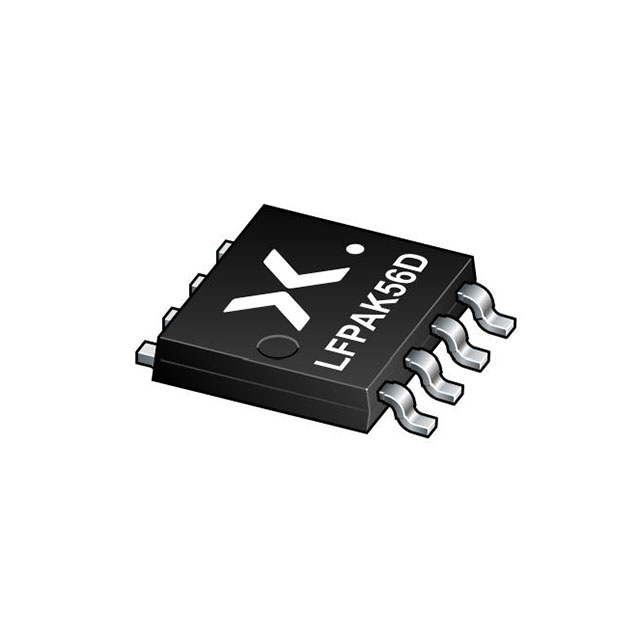
The BUK9K29-100E,115 is a dual N-channel TrenchMOS logic level MOSFET in an LFPAK56D (SOT1205) package. It features a drain-source voltage of 100 V and a continuous drain current of 30 A at 25 °C mounting base temperature. The typical on-state resistance is 25.1 mΩ at VGS = 5 V and ID = 5 A. Total gate charge is 54 nC. The device supports junction temperatures up to 175 °C and has a total power dissipation of 68 W.
Verify the specific ordering suffix
Select this component for designs requiring dual isolated channels in a compact surface-mount footprint. The logic level gate drive simplifies interface with standard microcontrollers or drivers. Ensure thermal management accounts for the 2.21 K/W junction-to-mounting-base resistance to maintain reliability within the specified temperature range.
This part belongs to Nexperia's BUK9 series of dual MOSFETs utilizing TrenchMOS technology. It is housed in the LFPAK56D package, also known as Dual Power-SO8. The device is designed specifically for automotive-grade reliability, meeting AEC-Q101 standards while offering high current handling capabilities suitable for power switching tasks.
Direct pin-compatible replacements include the BUK7K29-100EX and BUK7Y29-100E. Verify that alternative packages match the LFPAK56D/SOT1205 outline and confirm electrical parameters such as RDS(on) and Qg meet design requirements.
The maximum non-repetitive drain-source avalanche energy is 83 mJ when ID is 30 A, Vsup is less than or equal to 100 V, and the initial junction temperature is 25 °C.
The device maintains a true logic level gate with a VGS(th) rating greater than 0.5 V at a junction temperature of 175 °C.
The thermal resistance from junction to ambient is typically 95 K/W when mounted on a minimum footprint printed circuit board.
 BUK9K29-100E,115
The activity of extra discounts on wholesale prices is in full swing…
Please fill in your contact information and we will send you the latest wholesale price list.