 ChipApex | Global Electronic Components Supplier

SEARCH
Search Product
Search Post
— IC芯片 | 连接器 | 传感器 | 被动器件 —
Search productSearch post
— IC芯片 | 连接器 | 传感器 | 被动器件 —
Consult the customer manager about the wholesale price.
consultation hotline:86-132-6715-2157
email:[email protected]
Contact the product manager for consultation. One-stop consultation is available.
Do you want a lower wholesale price? Please send us your inquiry and we will reply immediately.
CD4021BCMX is listed in the Shift Registers range at ChipApex. The manufacturer field lists onsemi. Its product description is IC SHIFT REGISTER 8STAGE 16SOIC. Review the specifications below when checking this part for your BOM.
The CD4021BCMX is an 8-stage parallel input/serial output shift register manufactured by onsemi. It operates within a supply voltage range of 3.0V to 15V and supports operating temperatures from -55°C to +125°C. The device features symmetrical output characteristics with standard B series drive capabilities, high noise immunity at 0.45 VDD, and low power TTL compatibility. It includes static discharge protection diodes to VDD and VSS.
Verify the specific package configuration for the CD4021BCMX suffix, which indicates a tape and reel format. Confirm that the ordering code matches the required 16-lead Small Outline Integrated Circuit (SOIC) JEDEC MS-012 specification. Ensure the component meets the recommended operating conditions for the intended application environment.
Select this component when an 8-bit shift register with parallel load functionality is required in a compact surface-mount form factor. Consider the wide supply voltage range and high noise immunity for robust operation in electrically noisy environments. Verify that the SOIC package dimensions fit the available PCB space constraints.
This part belongs to the CD4000B series of CMOS logic devices, designed for general-purpose digital applications. It provides a reliable solution for data storage and transfer tasks where low power consumption and high noise immunity are critical requirements for system stability.
Compatible replacements include other 8-stage parallel-in serial-out shift registers from the CD4000B family, such as the CD4021BM or CD4021BCM, provided they match the SOIC-16 package and electrical specifications.
When the control input is logical '1', data is asynchronously jammed into each stage. When it is logical '0', data is serially shifted synchronously with the positive clock transition.
The recommended operating supply voltage range is 3.0V to 15V, with absolute maximum ratings extending up to 18V.
Explore related parts through Logic, Integrated Circuits (ICs), all product categories, ChipApex homepage.
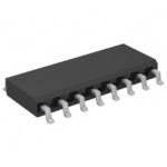 CD4021BCMX

CD4021BCMX is listed in the Shift Registers range at ChipApex. The manufacturer field lists onsemi. Its product description is IC SHIFT REGISTER 8STAGE 16SOIC.…
Read More
CD4021BCMX is listed in the Shift Registers range at ChipApex. The manufacturer field lists onsemi. Its product description is IC SHIFT REGISTER 8STAGE 16SOIC.…
Read More
CD4021BCMX is listed in the Shift Registers range at ChipApex. The manufacturer field lists onsemi. Its product description is IC SHIFT REGISTER 8STAGE 16SOIC.…
Read More
CD4021BCMX is listed in the Shift Registers range at ChipApex. The manufacturer field lists onsemi. Its product description is IC SHIFT REGISTER 8STAGE 16SOIC.…
Read More
CD4021BCMX is listed in the Shift Registers range at ChipApex. The manufacturer field lists onsemi. Its product description is IC SHIFT REGISTER 8STAGE 16SOIC.…
Read More
CD4021BCMX is listed in the Shift Registers range at ChipApex. The manufacturer field lists onsemi. Its product description is IC SHIFT REGISTER 8STAGE 16SOIC.…
Read More
CD4021BCMX is listed in the Shift Registers range at ChipApex. The manufacturer field lists onsemi. Its product description is IC SHIFT REGISTER 8STAGE 16SOIC.…
Read More
CD4021BCMX is listed in the Shift Registers range at ChipApex. The manufacturer field lists onsemi. Its product description is IC SHIFT REGISTER 8STAGE 16SOIC.…
Read More
CD4021BCMX is listed in the Shift Registers range at ChipApex. The manufacturer field lists onsemi. Its product description is IC SHIFT REGISTER 8STAGE 16SOIC.…
Read More
CD4021BCMX is listed in the Shift Registers range at ChipApex. The manufacturer field lists onsemi. Its product description is IC SHIFT REGISTER 8STAGE 16SOIC.…
Read More
CD4021BCMX is listed in the Shift Registers range at ChipApex. The manufacturer field lists onsemi. Its product description is IC SHIFT REGISTER 8STAGE 16SOIC.…
Read More
Compare thermistors, RTDs, thermocouples and temperature ICs. Learn how range, accuracy, response, interfaces and mounting affect component selection.
Read More
The activity of extra discounts on wholesale prices is in full swing…
Please fill in your contact information and we will send you the latest wholesale price list.





