ChipApex | Global Electronic Components Supplier
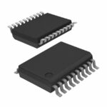
CLC5526MSAX/NOPB
Search Product
Search Post
— IC芯片 | 连接器 | 传感器 | 被动器件 —
Search productSearch post
— IC芯片 | 连接器 | 传感器 | 被动器件 —
Consult the customer manager about the wholesale price.
consultation hotline:86-132-6715-2157
email:[email protected]
Contact the product manager for consultation. One-stop consultation is available.
Do you want a lower wholesale price? Please send us your inquiry and we will reply immediately.
The CLC5526MSAX/NOPB is a high-performance, digitally controlled variable-gain amplifier (DVGA) from Texas Instruments. It features differential input and output with an input impedance of 200Ω and an output impedance of 600Ω. The device operates on a single +5V supply with a typical current consumption of 48 mA. It provides a wide gain range from -12 dB to +30 dB in 6 dB steps, controlled via a 3-bit parallel interface. The small-signal bandwidth is 350 MHz, maintaining this performance across the entire gain range. It includes internal clamping for fast overdrive recovery and supports TTL/CMOS logic compatibility.
Verify the specific suffix 'MSAX' against the manufacturer's official documentation to confirm package type and tape-and-reel specifications. Ensure the component meets RoHS compliance requirements as indicated by the NOPB designation. Confirm that the operating temperature range aligns with industrial standards (-40°C to +85°C). Validate pinout compatibility with existing PCB layouts before integration.
Select this component when a fixed-gain amplifier cannot accommodate varying signal levels in mixed-signal communication systems. The differential I/O simplifies interfacing with ADCs and other balanced circuits. Consider the 350 MHz bandwidth requirement and the need for precise digital gain stepping. Evaluate the power consumption constraints relative to the 48 mA typical draw and the availability of a +5V supply rail.
This part belongs to the CLC5526 family of digitally variable gain amplifiers designed for RF and IF applications. It serves as a key component in automatic gain control (AGC) loops to extend system dynamic range. The device integrates a resistive ladder and amplifier stages to provide accurate gain adjustments without external calibration.
Consult the manufacturer's product change notification database for officially confirmed substitute part numbers. Verify functional equivalence regarding gain range, bandwidth, and digital control interface before substitution.
The gain is set by a 3-bit parallel digital word, providing eight discrete steps ranging from -12 dB to +30 dB in 6 dB increments.
The LATCH pin controls whether the device operates in transparent mode, where gain changes immediately follow data inputs, or latched mode, where updates occur only on the rising edge of the latch signal.
While designed for differential outputs, it can drive single-ended loads if properly terminated, though differential driving is recommended for optimal performance and common-mode voltage stability.
 CLC5526MSAX/NOPB
The activity of extra discounts on wholesale prices is in full swing…
Please fill in your contact information and we will send you the latest wholesale price list.