 ChipApex | Global Electronic Components Supplier
SEARCH
Search Product
Search Post
— IC芯片 | 连接器 | 传感器 | 被动器件 —
Search productSearch post
— IC芯片 | 连接器 | 传感器 | 被动器件 —
Consult the customer manager about the wholesale price.
consultation hotline:86-132-6715-2157
email:[email protected]
Contact the product manager for consultation. One-stop consultation is available.
Do you want a lower wholesale price? Please send us your inquiry and we will reply immediately.
The CSD25301W1015 is a P-Channel NexFET Power MOSFET designed for ultra-low on-resistance and gate charge in a small footprint. It features a drain-to-source voltage of -20 V, continuous drain current of -2.2 A at 25°C, and an on-state resistance as low as 62 mΩ at VGS = -4.5V. The device utilizes a DSBGA-6 wafer-level package with dimensions of 1.0 x 1.5 mm and a maximum height of 0.62 mm. Operating junction temperature ranges from -55°C to +150°C.
Verify the specific ordering suffix matches the required media quantity and reel specifications. Confirm RoHS compliance status and halogen-free designation requirements against project standards. Ensure thermal design accounts for the specified RqJA values based on copper area constraints.
Select this component when minimizing board space is critical due to its 1x1.5 mm footprint. Evaluate thermal performance requirements against the provided RqJA limits for minimum versus full copper pad areas. Consider the low gate charge characteristics for high-frequency switching efficiency needs.
This part belongs to Texas Instruments' NexFET family of power MOSFETs. It is categorized under discrete semiconductor devices specifically engineered for power management and switching applications requiring compact form factors and high thermal efficiency.
CSD25211W1015
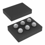 CSD25301W1015
The activity of extra discounts on wholesale prices is in full swing…
Please fill in your contact information and we will send you the latest wholesale price list.





