 ChipApex | Global Electronic Components Supplier
SEARCH
Search Product
Search Post
— IC芯片 | 连接器 | 传感器 | 被动器件 —
Search productSearch post
— IC芯片 | 连接器 | 传感器 | 被动器件 —
Consult the customer manager about the wholesale price.
consultation hotline:86-132-6715-2157
email:[email protected]
Contact the product manager for consultation. One-stop consultation is available.
Do you want a lower wholesale price? Please send us your inquiry and we will reply immediately.
The CSD75207W15 is a dual-channel P-Channel Power MOSFET from Texas Instruments, part of the NexFET family. It is housed in a compact 9DSBGA package designed for surface-mount applications. The device features a drain-source breakdown voltage (Vds) of 30 V and supports a continuous drain current (Id) of 3.9 A. Key electrical characteristics include a maximum on-resistance (Rds(on)) of 28 mΩ at Vgs = -4.5 V and 45 mΩ at Vgs = -2.5 V. The gate charge (Qg) is typically 6 nC at Vgs = -4.5 V, facilitating efficient switching performance.
Verify the specific ordering suffix and tape-and-reel specifications against the manufacturer's latest datasheet before procurement. Ensure compatibility with standard surface-mount assembly processes. Confirm RoHS compliance status and packaging quantity requirements directly with authorized distributors to align with production needs.
Select this component when a dual P-Channel solution is required in a minimal footprint. Evaluate the Rds(on) values at the intended gate drive voltage to ensure adequate conduction losses. Consider the thermal resistance of the 9DSBGA package relative to the expected power dissipation in the target application environment.
This device belongs to the CSD7520x series of NexFET power MOSFETs. It serves as a high-density alternative to discrete single-channel solutions, offering integrated functionality for dual-load control. The series is engineered for modern electronic designs prioritizing size reduction and energy efficiency.
Consult the official Texas Instruments selection guide for verified pin-compatible or functionally equivalent alternatives within the NexFET portfolio. Cross-reference package dimensions and electrical parameters to ensure seamless integration without circuit redesign.
The CSD75207W15 has a maximum drain-source voltage (Vds) rating of 30 V.
The device contains two independent P-Channel MOSFET channels within a single 9DSBGA package.
The typical total gate charge (Qg) is 6 nC when measured at a gate-source voltage of -4.5 V.
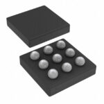 CSD75207W15
The activity of extra discounts on wholesale prices is in full swing…
Please fill in your contact information and we will send you the latest wholesale price list.





