ChipApex | Global Electronic Components Supplier
SEARCH
Search Product
Search Post
— IC芯片 | 连接器 | 传感器 | 被动器件 —
Search productSearch post
— IC芯片 | 连接器 | 传感器 | 被动器件 —
Consult the customer manager about the wholesale price.
consultation hotline:86-132-6715-2157
email:[email protected]
Contact the product manager for consultation. One-stop consultation is available.
Do you want a lower wholesale price? Please send us your inquiry and we will reply immediately.
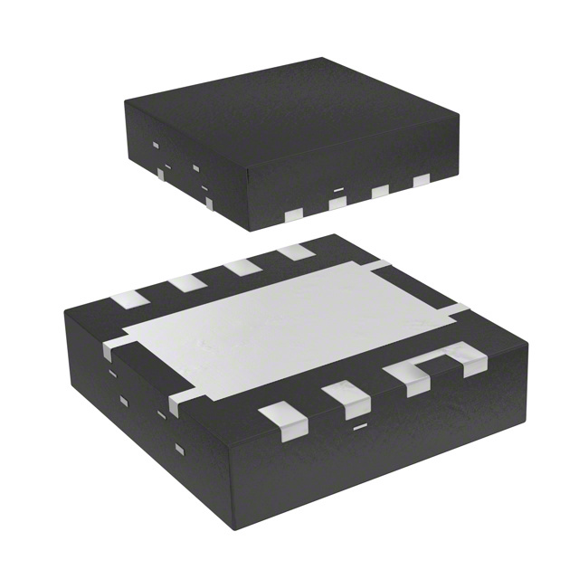
The CSD87334Q3DT is a NexFET power block from Texas Instruments, featuring an integrated P-channel MOSFET and dual N-channel MOSFETs in an 8-pin VSON package. It supports a maximum drain-source voltage of 30 V and delivers up to 60 A continuous current with an on-resistance of 8.3 mΩ. The device operates within a temperature range of -55 °C to +150 °C, dissipating up to 6 W of power. Key electrical parameters include a gate threshold voltage between 0.75 V and 1.2 V, a maximum gate-source voltage of -8 V/+10 V, and typical gate charge of 10.5 nC.
Verify the specific suffix 'DT' corresponds to the tape-and-reel packaging configuration required for automated assembly processes. Confirm that the component meets RoHS3 compliance standards and check the MSL rating for moisture sensitivity handling during storage and soldering. Ensure the ordering part number matches the exact NexFET power block variant to avoid pinout mismatches.
Select this component when designing synchronous rectification circuits requiring high current density and minimal board space. The integrated P-channel switch simplifies driver requirements compared to discrete solutions. Evaluate the 8.3 mΩ on-resistance against thermal constraints to ensure the 6 W power dissipation limit is not exceeded under peak load conditions.
This device belongs to the NexFET family, which integrates power transistors into single packages to reduce parasitic inductance and improve switching speeds. The CSD87334Q3DT specifically targets applications needing robust high-current handling in a small footprint, leveraging Texas Instruments' silicon carbide or advanced silicon process technologies for efficiency.
It contains one P-channel MOSFET and two N-channel MOSFETs configured as a half-bridge power block.
The device is optimized for applications with input voltages up to 24 V.
 CSD87334Q3DT
The activity of extra discounts on wholesale prices is in full swing…
Please fill in your contact information and we will send you the latest wholesale price list.