ChipApex | Global Electronic Components Supplier

SEARCH
Search Product
Search Post
— IC芯片 | 连接器 | 传感器 | 被动器件 —
Search productSearch post
— IC芯片 | 连接器 | 传感器 | 被动器件 —
Consult the customer manager about the wholesale price.
consultation hotline:86-132-6715-2157
email:[email protected]
Contact the product manager for consultation. One-stop consultation is available.
Do you want a lower wholesale price? Please send us your inquiry and we will reply immediately.
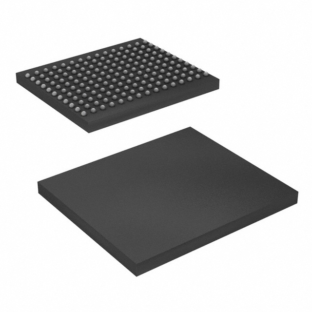
CY7C13451G-100BZXET is listed in the Memory IC range at ChipApex. The manufacturer field lists Infineon Technologies. Its product description is IC SRAM 4MBIT PAR 165FBGA. Review the specifications below when checking this part for your BOM.
The CY7C13451G-100BZXET is a 4-Mbit (128K × 36) synchronous flow-through static random-access memory manufactured by Infineon Technologies. It operates with a 3.3 V core supply and supports 2.5 V or 3.3 V I/O supplies. The device features an 8.0 ns maximum access time at a 100 MHz clock frequency, delivering high-performance 2-1-1-1 access rates. It utilizes a 165-ball FBGA package and includes user-selectable burst counter modes for Intel Pentium interleaved or linear burst sequences.
Verify the specific suffix 'E' corresponds to automotive qualification grades if required by your application environment. Confirm the 'T' suffix indicates tape-and-reel packaging rather than tray distribution. Ensure the 165-ball FBGA footprint matches your PCB design constraints. Cross-reference the latest datasheet revision for any errata regarding the ZZ pin connection requirements.
Select this component when a 36-bit data width is necessary for processor interfaces. The dual voltage capability allows compatibility with both 2.5 V and 3.3 V I/O logic levels. The synchronous flow-through architecture minimizes glue logic requirements compared to asynchronous alternatives. Consider the 165-ball FBGA package size against available board space and thermal dissipation capabilities.
This part belongs to the Cypress/Infineon CY7C13451G family of 4-Mbit synchronous SRAMs. It shares architectural similarities with other members in the Standard Sync series but is distinct in its 128K x 36 organization. The device represents a transition from older Cypress designs now maintained under Infineon Technologies.
Publicly confirmed substitute part numbers are not provided in the source material. Verify compatibility with existing designs before considering alternative vendors or pin-compatible upgrades.
The burst sequence is determined by the MODE input pin. A LOW selects a linear burst sequence, while a HIGH or floating state selects an interleaved burst sequence compatible with Intel Pentium processors.
The ZZ pin is an asynchronous input that places the device into a non-time critical sleep mode when asserted HIGH. Data integrity is preserved, and two clock cycles are required to enter or exit this mode.
Explore related parts through Memory, Integrated Circuits (ICs), all product categories, ChipApex homepage.
 CY7C13451G-100BZXET
CY7C13451G-100BZXET is listed in the Memory IC range at ChipApex. The manufacturer field lists Infineon Technologies. Its product description is IC SRAM 4MBIT PAR…
Read More
CY7C13451G-100BZXET is listed in the Memory IC range at ChipApex. The manufacturer field lists Infineon Technologies. Its product description is IC SRAM 4MBIT PAR…
Read More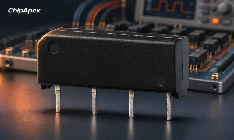
Choose a reed relay for signal switching. Understand hot and cold switching, leakage, contact resistance, isolation and measurement settling requirements.
Read More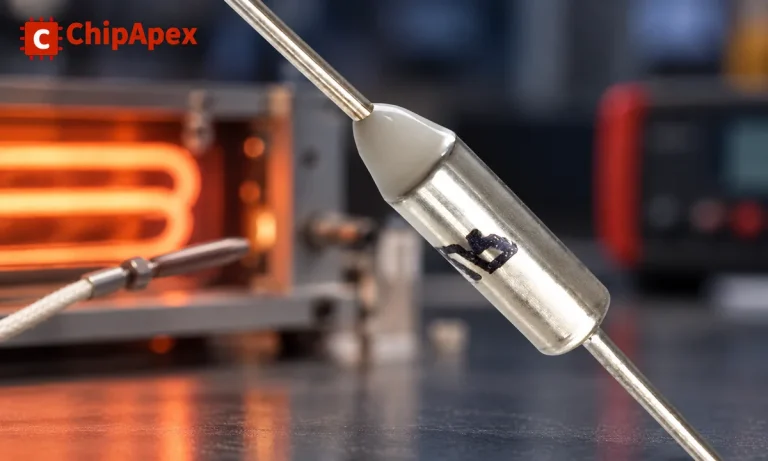
Understand thermal fuse operation, Tf, Th and Tm, electrical ratings and mounting. Check temperature limits and replacement requirements for your design.
Read More
CY7C13451G-100BZXET is listed in the Memory IC range at ChipApex. The manufacturer field lists Infineon Technologies. Its product description is IC SRAM 4MBIT PAR…
Read More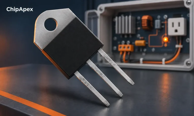
Learn how a TRIAC switches AC loads. Understand triggering, latching, holding current, phase control and thermal limits before choosing a component.
Read More
CY7C13451G-100BZXET is listed in the Memory IC range at ChipApex. The manufacturer field lists Infineon Technologies. Its product description is IC SRAM 4MBIT PAR…
Read More
CY7C13451G-100BZXET is listed in the Memory IC range at ChipApex. The manufacturer field lists Infineon Technologies. Its product description is IC SRAM 4MBIT PAR…
Read More
CY7C13451G-100BZXET is listed in the Memory IC range at ChipApex. The manufacturer field lists Infineon Technologies. Its product description is IC SRAM 4MBIT PAR…
Read More
CY7C13451G-100BZXET is listed in the Memory IC range at ChipApex. The manufacturer field lists Infineon Technologies. Its product description is IC SRAM 4MBIT PAR…
Read More
CY7C13451G-100BZXET is listed in the Memory IC range at ChipApex. The manufacturer field lists Infineon Technologies. Its product description is IC SRAM 4MBIT PAR…
Read More
CY7C13451G-100BZXET is listed in the Memory IC range at ChipApex. The manufacturer field lists Infineon Technologies. Its product description is IC SRAM 4MBIT PAR…
Read More
The activity of extra discounts on wholesale prices is in full swing…
Please fill in your contact information and we will send you the latest wholesale price list.