ChipApex | Global Electronic Components Supplier

SEARCH
Search Product
Search Post
— IC芯片 | 连接器 | 传感器 | 被动器件 —
Search productSearch post
— IC芯片 | 连接器 | 传感器 | 被动器件 —
Consult the customer manager about the wholesale price.
consultation hotline:86-132-6715-2157
email:[email protected]
Contact the product manager for consultation. One-stop consultation is available.
Do you want a lower wholesale price? Please send us your inquiry and we will reply immediately.
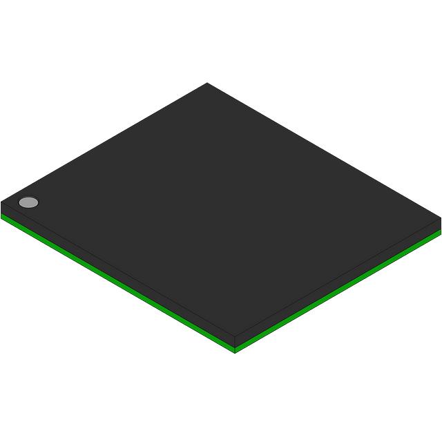
CY7C1484BV33-250BZXC is listed in the Memory IC range at ChipApex. The manufacturer field lists Cypress Semiconductor Corp. Its product description is IC SRAM 72MBIT PAR 165FBGA. Review the specifications below when checking this part for your BOM.
The CY7C1484BV33-250BZXC is a 72-Mbit (2 M × 36) pipelined synchronous SRAM from Cypress Semiconductor. It supports bus operations up to 250 MHz with a maximum access time of 3.0 ns. The device features registered inputs and outputs for pipelined operation, enabling high-performance double cycle deselect functionality. It operates with a 3.3 V core power supply and supports both 2.5 V and 3.3 V I/O levels. Key specifications include a maximum operating current of 500 mA and a maximum CMOS standby current of 120 mA.
Verify the specific speed grade corresponds to the 250 MHz requirement. Confirm that the 165-ball FBGA package matches the target PCB footprint. Ensure voltage compatibility with both 3.3 V core and 2.5/3.3 V I/O supplies. Check for Pb-free compliance if required by environmental standards. Validate JTAG boundary scan integration needs against the IEEE 1149.1 implementation details.
Select this component when a 72-Mbit capacity with a 36-bit data width is required. Choose this part for designs needing pipelined synchronous access at frequencies up to 250 MHz. Consider the dual voltage I/O capability if interfacing with mixed-voltage logic. Evaluate the double cycle deselect feature if minimizing latency during bank switching is critical for the application architecture.
This device belongs to the CY7C1484BV33 series of pipelined DCD Sync SRAMs. It is manufactured by Cypress Semiconductor Corporation. The component is housed in a Pb-free 165-ball FBGA package. It integrates advanced synchronous peripheral circuitry with a 2-bit counter for internal burst operation.
Consult official replacement guides for verified substitutes. Cross-reference pinouts and electrical characteristics carefully. Verify compatibility with existing system timing constraints before substitution.
The burst sequence is user-selectable via the MODE input pin. Tying MODE to GND selects a linear burst sequence, while leaving it floating or tying it to VDD selects an interleaved burst sequence.
The ZZ pin is an asynchronous sleep input. Asserting it HIGH places the device in a non-time-critical sleep mode to conserve power while preserving data integrity. Two clock cycles are required to enter or exit this mode.
Yes, the JTAG feature can be disabled by tying the TCK pin LOW. In this state, TDI and TMS may be left unconnected or pulled up, and TDO must be left unconnected.
Explore related parts through Memory, Integrated Circuits (ICs), all product categories, ChipApex homepage.
 CY7C1484BV33-250BZXC
Select a common mode choke using noise frequency, current, insulation and signal integrity. Understand impedance curves, layout and filter limitations.
Read More
CY7C1484BV33-250BZXC is listed in the Memory IC range at ChipApex. The manufacturer field lists Cypress Semiconductor Corp. Its product description is IC SRAM 72MBIT…
Read More
CY7C1484BV33-250BZXC is listed in the Memory IC range at ChipApex. The manufacturer field lists Cypress Semiconductor Corp. Its product description is IC SRAM 72MBIT…
Read More
CY7C1484BV33-250BZXC is listed in the Memory IC range at ChipApex. The manufacturer field lists Cypress Semiconductor Corp. Its product description is IC SRAM 72MBIT…
Read More
CY7C1484BV33-250BZXC is listed in the Memory IC range at ChipApex. The manufacturer field lists Cypress Semiconductor Corp. Its product description is IC SRAM 72MBIT…
Read More
CY7C1484BV33-250BZXC is listed in the Memory IC range at ChipApex. The manufacturer field lists Cypress Semiconductor Corp. Its product description is IC SRAM 72MBIT…
Read More
See when an inductor behaves linearly, how DC bias and saturation reduce inductance, and which current and temperature curves to check.
Read More
CY7C1484BV33-250BZXC is listed in the Memory IC range at ChipApex. The manufacturer field lists Cypress Semiconductor Corp. Its product description is IC SRAM 72MBIT…
Read More
CY7C1484BV33-250BZXC is listed in the Memory IC range at ChipApex. The manufacturer field lists Cypress Semiconductor Corp. Its product description is IC SRAM 72MBIT…
Read More
CY7C1484BV33-250BZXC is listed in the Memory IC range at ChipApex. The manufacturer field lists Cypress Semiconductor Corp. Its product description is IC SRAM 72MBIT…
Read More
CY7C1484BV33-250BZXC is listed in the Memory IC range at ChipApex. The manufacturer field lists Cypress Semiconductor Corp. Its product description is IC SRAM 72MBIT…
Read More
CY7C1484BV33-250BZXC is listed in the Memory IC range at ChipApex. The manufacturer field lists Cypress Semiconductor Corp. Its product description is IC SRAM 72MBIT…
Read More
The activity of extra discounts on wholesale prices is in full swing…
Please fill in your contact information and we will send you the latest wholesale price list.