 ChipApex | Global Electronic Components Supplier

SEARCH
Search Product
Search Post
— IC芯片 | 连接器 | 传感器 | 被动器件 —
Search productSearch post
— IC芯片 | 连接器 | 传感器 | 被动器件 —
Consult the customer manager about the wholesale price.
consultation hotline:86-132-6715-2157
email:[email protected]
Contact the product manager for consultation. One-stop consultation is available.
Do you want a lower wholesale price? Please send us your inquiry and we will reply immediately.
CY7C2565KV18-500BZXC is listed in the Memory IC range at ChipApex. The manufacturer field lists Cypress Semiconductor Corp. Its product description is IC SRAM 72MBIT PAR 165FBGA. Review the specifications below when checking this part for your BOM.
The CY7C2565KV18-500BZXC is a 72-Mbit QDR II+ Synchronous Pipelined SRAM with a 2M x 36 organization. It supports a maximum operating frequency of 500 MHz, providing high bandwidth through separate independent read and write data ports that allow concurrent transactions. The device features a 4-word burst architecture with 2.5 cycle read latency when the DOFF pin is asserted HIGH. It operates with a core voltage of 1.8V ± 0.1V and I/O voltages ranging from 1.4V to VDD. The component is housed in a 165-ball FBGA package measuring 13 x 15 x 1.4 mm.
Verify the specific speed grade suffix matches the required clock frequency, as the family includes variants up to 550 MHz. Confirm the package type corresponds to the 165-ball FBGA form factor. Ensure the supply voltage requirements align with the specified 1.8V core and 1.4V to 1.9V I/O ranges. Check for RoHS compliance status if environmental regulations apply to the target assembly process.
Select this component when a 72-Mbit capacity with a 36-bit data width is required for parallel interface applications. Choose this part over standard SRAMs when simultaneous read and write throughput is necessary without bus contention. Consider the QDR II+ architecture for designs needing echo clocks and on-die termination to simplify PCB routing and signal integrity management at frequencies up to 500 MHz.
This device belongs to the Cypress/Infineon QDR II+ SRAM family, which extends the QDR II specification by adding On-Die Termination capabilities. The family shares a common 165-ball FBGA footprint and functional architecture across various densities and widths. The CY7C2565KV18 specifically addresses the 2M x 36 configuration within this series, offering a balance between density and interface width for high-performance memory subsystems.
The CY7C2565KV18-550BZXC serves as a higher-speed variant within the same package and functional family. Verify compatibility if system timing margins require the 550 MHz rated version. No direct cross-manufacturer equivalents are documented in the provided source material.
When the DOFF pin is asserted HIGH, the device operates with a 2.5 cycle read latency using the PLL. When DOFF is LOW or connected to ground, the PLL is disabled, and the device behaves like a QDR I device with a 1 cycle read latency but longer access times.
The ZQ pin is used for output impedance matching. An external resistor (RQ) connected between ZQ and ground tunes the device outputs to the system data bus impedance. The output impedance is set to 0.2 times the value of RQ.
Explore related parts through Memory, Integrated Circuits (ICs), all product categories, ChipApex homepage.
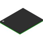 CY7C2565KV18-500BZXC
CY7C2565KV18-500BZXC is listed in the Memory IC range at ChipApex. The manufacturer field lists Cypress Semiconductor Corp. Its product description is IC SRAM 72MBIT…
Read More
Find out when a bare shock switch needs a pull resistor, when an MCU internal pull-up is enough, and why sensor modules and piezo…
Read More
CY7C2565KV18-500BZXC is listed in the Memory IC range at ChipApex. The manufacturer field lists Cypress Semiconductor Corp. Its product description is IC SRAM 72MBIT…
Read More
CY7C2565KV18-500BZXC is listed in the Memory IC range at ChipApex. The manufacturer field lists Cypress Semiconductor Corp. Its product description is IC SRAM 72MBIT…
Read More
CY7C2565KV18-500BZXC is listed in the Memory IC range at ChipApex. The manufacturer field lists Cypress Semiconductor Corp. Its product description is IC SRAM 72MBIT…
Read More
CY7C2565KV18-500BZXC is listed in the Memory IC range at ChipApex. The manufacturer field lists Cypress Semiconductor Corp. Its product description is IC SRAM 72MBIT…
Read More
CY7C2565KV18-500BZXC is listed in the Memory IC range at ChipApex. The manufacturer field lists Cypress Semiconductor Corp. Its product description is IC SRAM 72MBIT…
Read More
CY7C2565KV18-500BZXC is listed in the Memory IC range at ChipApex. The manufacturer field lists Cypress Semiconductor Corp. Its product description is IC SRAM 72MBIT…
Read More
CY7C2565KV18-500BZXC is listed in the Memory IC range at ChipApex. The manufacturer field lists Cypress Semiconductor Corp. Its product description is IC SRAM 72MBIT…
Read More
Learn how rectifiers convert AC to DC, compare half-wave and bridge circuits, and select voltage, current, recovery and thermal ratings for your design.
Read More
CY7C2565KV18-500BZXC is listed in the Memory IC range at ChipApex. The manufacturer field lists Cypress Semiconductor Corp. Its product description is IC SRAM 72MBIT…
Read More
CY7C2565KV18-500BZXC is listed in the Memory IC range at ChipApex. The manufacturer field lists Cypress Semiconductor Corp. Its product description is IC SRAM 72MBIT…
Read More
The activity of extra discounts on wholesale prices is in full swing…
Please fill in your contact information and we will send you the latest wholesale price list.





