 ChipApex | Global Electronic Components Supplier
SEARCH
Search Product
Search Post
— IC芯片 | 连接器 | 传感器 | 被动器件 —
Search productSearch post
— IC芯片 | 连接器 | 传感器 | 被动器件 —
Consult the customer manager about the wholesale price.
consultation hotline:86-132-6715-2157
email:[email protected]
Contact the product manager for consultation. One-stop consultation is available.
Do you want a lower wholesale price? Please send us your inquiry and we will reply immediately.
The DMC3730UVT-7 is a complementary pair enhancement mode MOSFET manufactured by Diodes Incorporated. It integrates an N-channel device (Q1) and a P-channel device (Q2) within a single TSOT26 package. The N-channel component provides a drain-source breakdown voltage of 25V, with maximum on-resistance values of 0.45Ω at VGS=4.5V, 0.60Ω at VGS=2.7V, and 0.73Ω at VGS=1.8V. The continuous drain current for the N-channel is 0.68A. The P-channel component features a -25V breakdown voltage, with maximum on-resistance values of 1.1Ω at VGS=-4.5V, 1.5Ω at VGS=-2.7V, and 2.2Ω at VGS=-1.8V. Its continuous drain current is rated at -0.46A.
Verify the specific ordering suffix against official documentation to confirm packaging quantity and reel specifications. Confirm RoHS compliance status and lead-free definitions directly from the manufacturer's quality documentation before procurement. Ensure the component meets AEC-Q101 reliability standards if automotive applications are intended.
Select this component when space-constrained designs require both high-side and low-side switching capabilities in a single footprint. Evaluate the thermal resistance characteristics against the expected power dissipation requirements. Consider the gate threshold voltage ranges to ensure compatibility with the driving logic levels used in the target application circuit.
This part belongs to the DMC3730 series of complementary MOSFETs produced by Diodes Incorporated. It utilizes silicon technology and is housed in a TSOT26 surface-mount case. The product is designed for high-efficiency power management applications requiring minimal on-state resistance while maintaining fast switching speeds.
Consult official cross-reference lists or datasheets for verified substitutes. Ensure any replacement maintains the same TSOT26 pinout configuration and matches the electrical ratings for both N-channel and P-channel devices.
The junction and storage temperature range is specified as -55°C to +175°C.
Yes, the device includes ESD protected gates and integrated gate protection diodes for both the N-channel and P-channel components.
The total power dissipation is rated at 0.7W under steady-state conditions on an FR-4 PC board with minimum recommended pad layout, and up to 0.9W with thermal bias to a bottom layer copper plate.
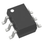 DMC3730UVT-7
The activity of extra discounts on wholesale prices is in full swing…
Please fill in your contact information and we will send you the latest wholesale price list.





