 ChipApex | Global Electronic Components Supplier
SEARCH
Search Product
Search Post
— IC芯片 | 连接器 | 传感器 | 被动器件 —
Search productSearch post
— IC芯片 | 连接器 | 传感器 | 被动器件 —
Consult the customer manager about the wholesale price.
consultation hotline:86-132-6715-2157
email:[email protected]
Contact the product manager for consultation. One-stop consultation is available.
Do you want a lower wholesale price? Please send us your inquiry and we will reply immediately.
The DMC62D2SV-7 is a complementary pair enhancement mode MOSFET manufactured by Diodes Incorporated in an SOT563 surface-mount package. It integrates an N-channel device (Q1) and a P-channel device (Q2). The N-channel transistor features a drain-source voltage of 60V, a maximum continuous drain current of 480mA at +25°C, and a static on-resistance of 1.7Ω at VGS=10V. The P-channel transistor has a -60V breakdown voltage, a -320mA continuous drain current, and a 4Ω on-resistance at VGS=-10V. Total power dissipation is rated at 0.5W with a thermal resistance of 261°C/W under steady-state conditions.
Verify the specific ordering suffix to confirm packaging quantity. The -7 suffix indicates a tape and reel carrier containing 3,000 units. Confirm that the required component meets all applicable automotive qualification standards if intended for such environments, as standard versions may differ from AEC-Q100 qualified parts.
Select this component when a compact dual-transistor solution is required for low-voltage signal routing or power control. Ensure the application current remains within the 480mA limit for the N-channel and 320mA for the P-channel at ambient temperatures near 25°C. Verify gate drive voltages align with the specified thresholds for optimal on-resistance performance.
This part belongs to the DMC62D series of complementary MOSFETs from Diodes Incorporated. It shares the same electrical characteristics and pinout as the DMC62D0SV, differing primarily in the manufacturing date code marking scheme associated with its specific production run.
DMC62D0SV-7
The maximum operating and storage temperature range extends up to +150°C.
The on-resistance increases as the junction temperature rises, as illustrated in the typical on-resistance versus junction temperature graphs provided in the datasheet.
Yes, the reverse recovery time is specified as 19ns for the N-channel and 26.6ns for the P-channel at specific test currents.
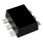 DMC62D2SV-7
The activity of extra discounts on wholesale prices is in full swing…
Please fill in your contact information and we will send you the latest wholesale price list.





