 ChipApex | Global Electronic Components Supplier
SEARCH
Search Product
Search Post
— IC芯片 | 连接器 | 传感器 | 被动器件 —
Search productSearch post
— IC芯片 | 连接器 | 传感器 | 被动器件 —
Consult the customer manager about the wholesale price.
consultation hotline:86-132-6715-2157
email:[email protected]
Contact the product manager for consultation. One-stop consultation is available.
Do you want a lower wholesale price? Please send us your inquiry and we will reply immediately.
The DMG6602SVT is a complementary pair enhancement mode MOSFET in a TSOT26 package, containing an N-channel Q1 and P-channel Q2. Q1 offers a 30V drain-source voltage with on-resistance of 60mΩ at VGS=10V (ID=3.4A) and 100mΩ at VGS=4.5V (ID=2.7A). Q2 provides -30V breakdown with 95mΩ at VGS=-10V (ID=-2.8A) and 140mΩ at VGS=-4.5V (ID=-2.3A). The device supports continuous currents up to 3.4A for Q1 and 2.8A for Q2 at +25°C, with pulsed capabilities of 25A and 20A respectively. It operates within a junction temperature range of -55°C to +150°C.
Verify component authenticity through authorized Diodes Incorporated distributors or direct channels. Confirm the part number matches DMG6602SVT-7 for tape and reel packaging. Check for RoHS compliance and lead-free status as specified in the datasheet notes. Ensure storage conditions adhere to moisture sensitivity level 1 requirements to prevent package damage during soldering processes.
Select this component for applications requiring a compact complementary MOSFET pair in a TSOT26 footprint. Evaluate thermal performance based on the specific PCB copper area and ambient temperature conditions. Consider the gate threshold voltage and drive voltage levels to ensure optimal RDS(on) performance for both N-channel and P-channel devices in the target circuit design.
This component is identified as not recommended for new design by the manufacturer. The datasheet explicitly recommends using the DMC3071LVT as a replacement. This status indicates that while the part remains functional for existing designs, it is no longer the preferred choice for new product development due to potential availability or updated technology alternatives.
The official replacement specified in the datasheet is the DMC3071LVT. Verify pin compatibility and electrical parameters against the original design requirements before substitution. Ensure the alternative component meets the same package size and thermal characteristics if space constraints are critical.
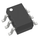 DMG6602SVT-7
The activity of extra discounts on wholesale prices is in full swing…
Please fill in your contact information and we will send you the latest wholesale price list.





