 ChipApex | Global Electronic Components Supplier

SEARCH
Search Product
Search Post
— IC芯片 | 连接器 | 传感器 | 被动器件 —
Search productSearch post
— IC芯片 | 连接器 | 传感器 | 被动器件 —
Consult the customer manager about the wholesale price.
consultation hotline:86-132-6715-2157
email:[email protected]
Contact the product manager for consultation. One-stop consultation is available.
Do you want a lower wholesale price? Please send us your inquiry and we will reply immediately.
The DMN33D9LV-7 is a dual N-channel enhancement mode MOSFET manufactured by Diodes Incorporated in an SOT563 surface-mount package. It features a drain-source voltage (BVDSS) of 30V and a continuous drain current (ID) of 350mA at +25°C. The maximum on-resistance (RDS(ON)) is specified as 2.4Ω at VGS=10V, 3.0Ω at VGS=4.5V, and 7.0Ω at VGS=2.5V. Total gate charge (Qg) reaches 1.23nC at VGS=10V. Operating temperature ranges from -55°C to +150°C with a power dissipation of 430mW.
Verify the specific ordering suffix against official documentation to confirm reel size and marking variations. Confirm RoHS compliance status and moisture sensitivity level requirements prior to procurement. Ensure storage conditions align with J-STD-020 standards to prevent damage before soldering.
Select this component for applications requiring dual N-channel control within a minimal footprint. Evaluate RDS(ON) performance at the specific operating gate voltage to ensure efficiency targets are met. Consider thermal constraints given the 430mW power dissipation limit in the SOT563 package.
This device belongs to the DMN33 series of dual N-channel MOSFETs designed for low-voltage power management. It utilizes silicon technology and is housed in a molded plastic SOT563 case. The product is lead-free and halogen/antimony free, adhering to environmental directives.
Check for pin-compatible alternatives within the same manufacturer's portfolio that match the 30V BVDSS and SOT563 form factor. Verify electrical parameters such as RDS(ON) and Qg to ensure equivalent switching performance. No official substitute part numbers are documented in the provided datasheet.
The maximum continuous drain current is 350mA at an ambient temperature of +25°C.
For automotive applications requiring AEC-Q100/101/200 qualification or IATF 16949 manufacturing, contact Diodes Incorporated directly as standard parts may not meet these specific controls.
The gate threshold voltage (VGS(TH)) ranges from a minimum of 0.8V to a maximum of 1.4V under test conditions of VDS=3V and ID=100μA.
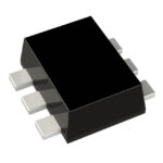 DMN33D9LV-7

The activity of extra discounts on wholesale prices is in full swing…
Please fill in your contact information and we will send you the latest wholesale price list.





