 ChipApex | Global Electronic Components Supplier

SEARCH
Search Product
Search Post
— IC芯片 | 连接器 | 传感器 | 被动器件 —
Search productSearch post
— IC芯片 | 连接器 | 传感器 | 被动器件 —
Consult the customer manager about the wholesale price.
consultation hotline:86-132-6715-2157
email:[email protected]
Contact the product manager for consultation. One-stop consultation is available.
Do you want a lower wholesale price? Please send us your inquiry and we will reply immediately.
The DMN52D0UVA-13 is a dual N-channel enhancement mode MOSFET manufactured by Diodes Incorporated. It features a maximum drain-source voltage (BVDSS) of 50V and a gate-source voltage rating of ±12V. The device offers low on-resistance, with maximum values of 4Ω at VGS=1.8V, 2.5Ω at VGS=2.5V, and 2Ω at VGS=5V. Continuous drain current reaches 480mA at +25°C. Total gate charge is 0.8nC at VGS=4.5V. Operating temperature ranges from -55°C to +150°C.
Verify the specific ordering suffix when purchasing. The -13 suffix indicates a reel packing quantity of 10,000 units. Confirm that the required packaging format aligns with automated assembly equipment specifications before placing orders to ensure compatibility with production lines.
Select this component for applications requiring a compact dual N-channel solution with low on-resistance. Ensure the operating gate-source voltage meets the minimum threshold requirements for the desired load current. Verify thermal dissipation capabilities against the junction-to-ambient resistance values provided in the datasheet for the specific PCB layout.
This part belongs to the DMN52 series of dual N-channel MOSFETs from Diodes Incorporated. The series is designed to minimize on-state resistance while maintaining superior switching performance. Other variants in the family include different packaging options or slight electrical parameter variations, all sharing the core 50V N-channel enhancement mode architecture.
Direct substitutes within the same product line include the DMN52D0UVA-7, which shares identical electrical characteristics but utilizes a 3,000-unit reel packaging format. When evaluating alternative components, verify pinout compatibility and ensure equivalent breakdown voltage and on-resistance specifications are met.
The maximum continuous drain current is 480mA at an ambient temperature of +25°C.
For automotive applications requiring specific change control, AEC-Q100/101/104/200 qualification, PPAP capability, and manufacturing in IATF 16949 certified facilities, customers must contact Diodes Incorporated directly.
The typical total gate charge is 0.8nC when tested at VDS = 25V and ID = 50mA.
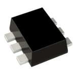 DMN52D0UVA-13

The activity of extra discounts on wholesale prices is in full swing…
Please fill in your contact information and we will send you the latest wholesale price list.





