 ChipApex | Global Electronic Components Supplier

SEARCH
Search Product
Search Post
— IC芯片 | 连接器 | 传感器 | 被动器件 —
Search productSearch post
— IC芯片 | 连接器 | 传感器 | 被动器件 —
Consult the customer manager about the wholesale price.
consultation hotline:86-132-6715-2157
email:[email protected]
Contact the product manager for consultation. One-stop consultation is available.
Do you want a lower wholesale price? Please send us your inquiry and we will reply immediately.
The DMN5L06DWK-7 is a dual N-channel enhancement mode MOSFET manufactured by Diodes Incorporated. It features a maximum drain-source voltage (VDSS) of 50V and a continuous drain current (ID) of 305mA at 25°C. The device has a gate-source threshold voltage (VGS(TH)) of 1.0V maximum at 250µA. Static drain-source on-resistance (RDS(ON)) is specified as 2.0Ω at VGS=5.0V and ID=50mA, 2.5Ω at VGS=2.5V, and 3.0Ω at VGS=1.8V. Total power dissipation is 250mW at 25°C with a thermal resistance of 500°C/W. Operating temperature ranges from -65°C to +150°C.
Verify the component datasheet revision number against the manufacturer's official documentation before integration. Confirm that the SOT363 package dimensions match the target PCB footprint requirements. Ensure design compliance with the stated absolute maximum ratings, particularly regarding thermal resistance and junction temperature limits during operation.
Select this component for designs requiring a compact dual N-channel solution with low gate drive requirements. Evaluate the 250mW power dissipation limit relative to the expected load current and ambient temperature conditions. Consider the 50V breakdown voltage rating when designing for higher voltage environments.
This part belongs to the DMN5L06 series of dual N-channel enhancement mode MOSFETs produced by Diodes Incorporated. It utilizes the SOT363 case style, which provides a compact form factor suitable for space-constrained printed circuit board layouts. The device is designed for general-purpose switching and amplification tasks.
The datasheet explicitly states that this part is not recommended for new designs and recommends using DMN61D9UDW as the replacement.
The maximum gate-source voltage (VGSS) is ±20V.
Yes, the device is qualified to AEC-Q101 standards for high reliability.
The typical input capacitance (Ciss) is 50pF at VDS=25V and VGS=0V.
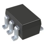 DMN5L06DWK-7

The activity of extra discounts on wholesale prices is in full swing…
Please fill in your contact information and we will send you the latest wholesale price list.





