 ChipApex | Global Electronic Components Supplier

SEARCH
Search Product
Search Post
— IC芯片 | 连接器 | 传感器 | 被动器件 —
Search productSearch post
— IC芯片 | 连接器 | 传感器 | 被动器件 —
Consult the customer manager about the wholesale price.
consultation hotline:86-132-6715-2157
email:[email protected]
Contact the product manager for consultation. One-stop consultation is available.
Do you want a lower wholesale price? Please send us your inquiry and we will reply immediately.
The DMN5L06VK-7-G is a dual N-channel enhancement mode MOSFET manufactured by Diodes Incorporated. It features a maximum drain-source voltage (V_DSS) of 50 V and a continuous drain current (I_D) of 280 mA at 25°C. The device offers a low gate threshold voltage with a maximum value of 1.0 V. Static drain-source on-resistance (R_DS(ON)) ranges from 2.0 Ω to 3.0 Ω depending on the gate-source voltage and drain current conditions. Total power dissipation is rated at 250 mW, with an operating temperature range spanning from -55°C to +150°C.
Verify that the specific ordering suffix matches the required packing quantity and pin 1 indicator marking. Confirm compliance with RoHS and halogen-free standards if environmental regulations apply to the assembly process. Ensure the design accounts for the component's status as not recommended for new designs by consulting the manufacturer's latest recommendations.
Select this component when a compact dual N-channel solution is required for low-voltage logic interfacing. Evaluate the thermal resistance and power dissipation limits relative to the expected ambient temperature and PCB copper area. Consider the low gate threshold voltage compatibility with standard logic levels while verifying the on-resistance meets the specific current handling requirements.
This part belongs to the DMN5/L06VK family of dual N-channel enhancement mode MOSFETs. It utilizes a SOT563 package constructed with a molded plastic compound. The device is designed for high reliability and is qualified to JEDEC standards. It serves as a space-efficient alternative for single-channel applications requiring two switches within a minimal footprint.
The datasheet explicitly recommends using the DMN52D0UV and DMN52D0UVA as replacements for new designs.
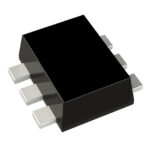 DMN5L06VK-7-G

The activity of extra discounts on wholesale prices is in full swing…
Please fill in your contact information and we will send you the latest wholesale price list.





