 ChipApex | Global Electronic Components Supplier

SEARCH
Search Product
Search Post
— IC芯片 | 连接器 | 传感器 | 被动器件 —
Search productSearch post
— IC芯片 | 连接器 | 传感器 | 被动器件 —
Consult the customer manager about the wholesale price.
consultation hotline:86-132-6715-2157
email:[email protected]
Contact the product manager for consultation. One-stop consultation is available.
Do you want a lower wholesale price? Please send us your inquiry and we will reply immediately.
The DMN62D0UDW-13 is a dual N-channel enhancement mode MOSFET manufactured by Diodes Incorporated. It features a maximum drain-source voltage (BVDSS) of 60V and a gate-source voltage (VGSS) rating of ±20V. The device offers a maximum static drain-source on-resistance (RDS(on)) of 2.0Ω at VGS = 4.5V and 2.5Ω at VGS = 2.5V. Continuous drain current (ID) is rated at 350mA at +25°C and 290mA at +70°C. Total power dissipation (PD) reaches 320mW on FR-4 PCB with minimum pad layout, or 410mW on high copper coverage boards. Operating temperature range spans from -55°C to +150°C.
Verify the specific ordering suffix '-13' corresponds to the 10,000-unit tape and reel packaging format. Confirm that the standard case material meets UL flammability classification 94V-0 requirements for your assembly process. Ensure compatibility with J-STD-020 moisture sensitivity level 1 handling procedures during storage and reflow soldering.
Select this component when a compact dual N-channel solution is required for low-voltage switching tasks. The SOT363 package provides space savings compared to larger transistor packages. Evaluate thermal resistance parameters against your PCB copper area to ensure junction temperatures remain within the specified operating range under continuous load conditions.
This part belongs to the DMN62D0U series of dual N-channel MOSFETs designed for portable and battery-powered electronics. It serves as a complementary switch pair within a single footprint, reducing board space and simplifying bill of materials. The device utilizes silicon technology and is intended for general-purpose commercial applications rather than automotive-grade environments.
For automotive applications requiring specific change control, refer to the related automotive grade part with the Q-suffix designation. Verify pinout compatibility if substituting with other dual N-channel devices in the SOT363 package.
The continuous drain current decreases to 290mA when the ambient temperature reaches +70°C.
Total power dissipation is rated at 320mW on FR-4 PCB with minimum recommended pad layout, and increases to 410mW on a 1” x 1” FR-4 PCB with high coverage 2oz copper.
Yes, the part is qualified to JEDEC standards for high reliability, though it is not explicitly designated for automotive AEC-Q qualification without the Q-suffix.
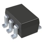 DMN62D0UDW-13

The activity of extra discounts on wholesale prices is in full swing…
Please fill in your contact information and we will send you the latest wholesale price list.





