 ChipApex | Global Electronic Components Supplier

SEARCH
Search Product
Search Post
— IC芯片 | 连接器 | 传感器 | 被动器件 —
Search productSearch post
— IC芯片 | 连接器 | 传感器 | 被动器件 —
Consult the customer manager about the wholesale price.
consultation hotline:86-132-6715-2157
email:[email protected]
Contact the product manager for consultation. One-stop consultation is available.
Do you want a lower wholesale price? Please send us your inquiry and we will reply immediately.
The DMP2100UCB9-7 is a dual P-channel enhancement mode MOSFET designed for high-efficiency power management. It features an 80mΩ typical on-state resistance at VGS = -4.5V and supports a continuous drain current of -4A. The device utilizes LD-MOS technology to minimize on-state losses while maintaining ultra-fast switching performance with a total gate charge of 3.3nC. It operates within a junction temperature range of -55°C to +150°C and includes 3kV HBM ESD protection.
Verify the component against the official Diodes Incorporated datasheet DS35725 Rev. 5-2 to confirm authenticity. Ensure the package matches the U-WLB1515-9 specification. Confirm compliance with RoHS directives and AEC-Q101 standards as documented in the manufacturer's release notes.
Select this component for applications requiring compact dual P-channel configurations. The low profile height and small footprint suit space-constrained designs. Evaluate thermal requirements based on the specific PCB copper area, as power dissipation varies significantly between minimum pad layouts and larger ground planes.
This part belongs to the DMP series of dual P-channel MOSFETs from Diodes Incorporated. It is packaged in the U-WLB1515-9 case, which measures 1.5mm by 1.5mm. The device is supplied in tape and reel packaging for automated surface-mount assembly processes.
Consult the manufacturer's documentation for qualified alternatives. Verify that any substitute maintains the same voltage ratings, current capabilities, and package dimensions to ensure mechanical and electrical compatibility.
The maximum pulsed drain current is -28A with a pulse duration of 10μs and a duty cycle of 1% or less.
Yes, the DMP2100UCB9 is qualified to AEC-Q101 standards for high reliability.
The typical gate threshold voltage is -0.7V at a drain-source voltage equal to the gate-source voltage with a drain current of -250μA.
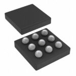 DMP2100UCB9-7

The activity of extra discounts on wholesale prices is in full swing…
Please fill in your contact information and we will send you the latest wholesale price list.





