 ChipApex | Global Electronic Components Supplier

SEARCH
Search Product
Search Post
— IC芯片 | 连接器 | 传感器 | 被动器件 —
Search productSearch post
— IC芯片 | 连接器 | 传感器 | 被动器件 —
Consult the customer manager about the wholesale price.
consultation hotline:86-132-6715-2157
email:[email protected]
Contact the product manager for consultation. One-stop consultation is available.
Do you want a lower wholesale price? Please send us your inquiry and we will reply immediately.
The DMP2110UVT-7 is a dual P-channel enhancement mode MOSFET manufactured by Diodes Incorporated in a TSOT26 package. It features a drain-source voltage (V_DSS) of -20 V and continuous drain current (I_D) of -1.8 A at +25°C. The maximum on-resistance (R_DS(ON)) is 150 mΩ at V_GS = -4.5 V, 200 mΩ at -2.5 V, and 240 mΩ at -1.8 V. Gate threshold voltage (V_GS(TH)) ranges from -0.45 V to -1.0 V. Input capacitance (C_iss) is typically 443 pF, with total gate charge (Q_g) at 6.0 nC. Operating temperature spans -55°C to +150°C.
Verify the specific ordering suffix against official documentation to confirm packaging quantity and reel specifications. Confirm that the component meets required environmental compliance standards such as RoHS and halogen-free definitions. Ensure the selected variant matches the intended thermal and electrical requirements for the target application design.
Select this component based on the requirement for dual P-channel isolation in a minimal footprint. Evaluate the R_DS(ON) values at specific gate drive voltages to ensure adequate efficiency. Consider the thermal resistance characteristics and package limitations when designing for continuous or pulsed current loads.
This device belongs to the DMP series of dual P-channel MOSFETs from Diodes Incorporated. It utilizes a TSOT26 case style designed for surface mount technology. The product line focuses on minimizing on-resistance while maintaining fast switching speeds for modern electronic systems.
Consult official manufacturer substitution guides for verified alternatives. Cross-reference pinouts, electrical ratings, and package dimensions before implementation.
The maximum continuous drain current is -1.8 A at an ambient temperature of +25°C.
The DMP2110UVT integrates two independent P-channel MOSFET channels.
The typical input capacitance (C_iss) is 443 pF under specified test conditions.
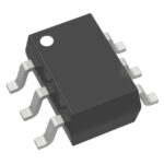 DMP2110UVT-7

The activity of extra discounts on wholesale prices is in full swing…
Please fill in your contact information and we will send you the latest wholesale price list.





