 ChipApex | Global Electronic Components Supplier

SEARCH
Search Product
Search Post
— IC芯片 | 连接器 | 传感器 | 被动器件 —
Search productSearch post
— IC芯片 | 连接器 | 传感器 | 被动器件 —
Consult the customer manager about the wholesale price.
consultation hotline:86-132-6715-2157
email:[email protected]
Contact the product manager for consultation. One-stop consultation is available.
Do you want a lower wholesale price? Please send us your inquiry and we will reply immediately.
The DMS3017SSD-13 is an asymmetric dual N-channel enhancement mode MOSFET in an SO-8 package. It integrates a Schottky diode on one die to minimize conduction and switching losses. Q1 features a typical RDS(on) of 8.5 mΩ at VGS=10V and 9.5 mΩ at VGS=4.5V, with a continuous drain current of 8.0A at 25°C. Q2 has a typical RDS(on) of 15 mΩ at VGS=10V and 25 mΩ at VGS=4.5V, with a continuous drain current of 6.0A at 25°C. Both channels support a VDSS of 30V and operate within a temperature range of -55°C to +150°C.
Verify the specific ordering suffix '-13' corresponds to the tape and reel packaging configuration required for your assembly line. Confirm that the SO-8 case dimensions align with your PCB footprint specifications. Ensure the component meets RoHS and halogen-free requirements if mandated by your project standards. Check for any end-of-life notices as the datasheet indicates it may not be recommended for new designs.
Select this component when an asymmetric dual MOSFET solution is needed to save board space and simplify driver requirements. The integrated Schottky diode on Q1 offers lower forward voltage compared to standard body diodes, improving efficiency in synchronous rectification. Consider the thermal resistance values based on your specific PCB copper coverage and airflow conditions to ensure adequate heat dissipation.
This device belongs to Diodes Incorporated's DIOFET family, which utilizes a patented process to integrate discrete components. The DMS3017SSD-13 specifically targets applications requiring compact, high-reliability power switching solutions. It is designed to replace multiple discrete components, reducing system complexity and potential failure points in power management designs.
The datasheet explicitly states 'NOT RECOMMENDED FOR NEW DESIGN' and 'NO ALTERNATE PRODUCT'. No public substitute part numbers are confirmed for direct replacement. Designers should evaluate newer asymmetric MOSFET families from the manufacturer or other suppliers if this component is no longer suitable for new projects.
Q1 is the primary channel with lower on-resistance (8.5 mΩ typ) and higher current capability (8.0A), while Q2 is the secondary channel with higher on-resistance (15 mΩ typ) and lower current capability (6.0A). Q1 also includes an integrated Schottky diode.
Yes, the device is qualified to AEC-Q101 standards, making it suitable for high-reliability automotive electronics applications.
The integrated Schottky diode on Q1 reduces the forward voltage drop and reverse recovery charge (Qrr) compared to a standard body diode, thereby minimizing switching losses during operation.
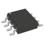 DMS3017SSD-13

The activity of extra discounts on wholesale prices is in full swing…
Please fill in your contact information and we will send you the latest wholesale price list.





