ChipApex | Global Electronic Components Supplier

SEARCH
Search Product
Search Post
— IC芯片 | 连接器 | 传感器 | 被动器件 —
Search productSearch post
— IC芯片 | 连接器 | 传感器 | 被动器件 —
Consult the customer manager about the wholesale price.
consultation hotline:86-132-6715-2157
email:[email protected]
Contact the product manager for consultation. One-stop consultation is available.
Do you want a lower wholesale price? Please send us your inquiry and we will reply immediately.
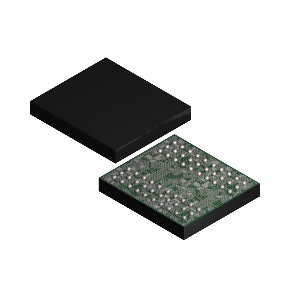
EMD28164PCH-60-SU is listed in the Memory IC range at ChipApex. The manufacturer field lists Jeju Semiconductor Corp. Its product description is 128M LPDDR1 PKG 8x9mm 60B BGA. Review the specifications below when checking this part for your BOM.
The EMD28164PCH-60-SU is a 128Mb Mobile DDR SDRAM fabricated using high-performance CMOS technology. It features a x16 data width and operates with VDD/VDDQ supply voltages between 1.7V and 1.95V. The device supports clock rates of 200MHz, 166MHz, and 133MHz. It utilizes a double data rate architecture with four internal banks for concurrent operation. Key specifications include CAS latencies of 2 and 3, burst lengths of 2, 4, 8, and 16, and a 64ms refresh period. The interface uses LVCMOS signaling.
Verify the specific speed grade suffix matches the required operating frequency (200MHz, 166MHz, or 133MHz) as indicated in the part number structure. Confirm that the package type corresponds to the 60-ball FPBGA assignment detailed in the datasheet. Ensure compatibility with the specified 1.7V to 1.95V operating voltage range for both core and I/O supplies.
Select this component for designs requiring a 128Mb capacity with a x16 interface width. Consider the available CAS latency options of 2 and 3 based on timing requirements. Evaluate the need for PASR and ATCSR features if power management during self-refresh is critical. Ensure the system supports the initialization sequence involving two auto-refresh commands before normal operation.
This device belongs to the Mobile DDR SDRAM family, designed for mobile and high-performance applications. It employs a 2n-prefetch architecture to achieve high-speed data transfer at the I/O balls. The organization consists of four banks, each containing 33,554,432 bits arranged as 4,096 rows by 512 columns by 16 bits.
Public confirmed substitute part numbers are not available in the provided documentation.
The device requires power-up, stable clocks, a PRECHARGE ALL command, two AUTO REFRESH commands, and programming of both the Mode Register and Extended Mode Register before it is ready for valid commands.
DM is an input mask signal for write data. Input data is masked when DM is sampled HIGH along with that input data during a WRITE access. DM is sampled on both edges of DQS.
Explore related parts through Memory, Integrated Circuits (ICs), all product categories, ChipApex homepage.
 EMD28164PCH-60-SU

EMD28164PCH-60-SU is listed in the Memory IC range at ChipApex. The manufacturer field lists Jeju Semiconductor Corp. Its product description is 128M LPDDR1 PKG…
Read More
Choose logic inverter ICs by thresholds, supply, output drive and delay. Compare standard and Schmitt-trigger inputs, power sequencing and replacement checks.
Read More
EMD28164PCH-60-SU is listed in the Memory IC range at ChipApex. The manufacturer field lists Jeju Semiconductor Corp. Its product description is 128M LPDDR1 PKG…
Read More
EMD28164PCH-60-SU is listed in the Memory IC range at ChipApex. The manufacturer field lists Jeju Semiconductor Corp. Its product description is 128M LPDDR1 PKG…
Read More
EMD28164PCH-60-SU is listed in the Memory IC range at ChipApex. The manufacturer field lists Jeju Semiconductor Corp. Its product description is 128M LPDDR1 PKG…
Read More
EMD28164PCH-60-SU is listed in the Memory IC range at ChipApex. The manufacturer field lists Jeju Semiconductor Corp. Its product description is 128M LPDDR1 PKG…
Read More
EMD28164PCH-60-SU is listed in the Memory IC range at ChipApex. The manufacturer field lists Jeju Semiconductor Corp. Its product description is 128M LPDDR1 PKG…
Read More
Compare RC, crystal and MEMS oscillator circuits. Check ppm, jitter, load capacitance, startup margin and output compatibility before choosing a clock source.
Read More
EMD28164PCH-60-SU is listed in the Memory IC range at ChipApex. The manufacturer field lists Jeju Semiconductor Corp. Its product description is 128M LPDDR1 PKG…
Read More
EMD28164PCH-60-SU is listed in the Memory IC range at ChipApex. The manufacturer field lists Jeju Semiconductor Corp. Its product description is 128M LPDDR1 PKG…
Read More
EMD28164PCH-60-SU is listed in the Memory IC range at ChipApex. The manufacturer field lists Jeju Semiconductor Corp. Its product description is 128M LPDDR1 PKG…
Read More
EMD28164PCH-60-SU is listed in the Memory IC range at ChipApex. The manufacturer field lists Jeju Semiconductor Corp. Its product description is 128M LPDDR1 PKG…
Read More
The activity of extra discounts on wholesale prices is in full swing…
Please fill in your contact information and we will send you the latest wholesale price list.