ChipApex | Global Electronic Components Supplier

SEARCH
Search Product
Search Post
— IC芯片 | 连接器 | 传感器 | 被动器件 —
Search productSearch post
— IC芯片 | 连接器 | 传感器 | 被动器件 —
Consult the customer manager about the wholesale price.
consultation hotline:86-132-6715-2157
email:[email protected]
Contact the product manager for consultation. One-stop consultation is available.
Do you want a lower wholesale price? Please send us your inquiry and we will reply immediately.
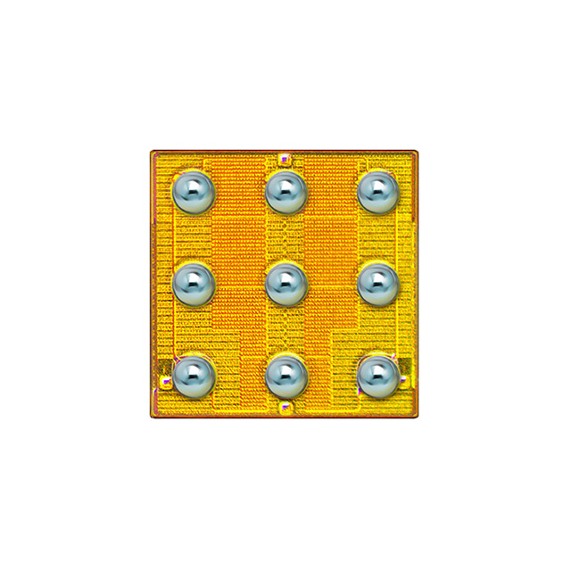
EPC2110 is listed in the FET, MOSFET Arrays range at ChipApex. The manufacturer field lists EPC. Its product description is MOSFET 2N-CH 120V 3.4A DIE. Review the specifications below when checking this part for your BOM.
The EPC2110 is a dual common-source enhancement-mode gallium nitride (GaN) power transistor featuring two independent N-channel devices within a single die. It offers a drain-to-source voltage rating of 120 V and a continuous drain current of 3.4 A at 25°C, with a maximum on-resistance of 110 mΩ. The device utilizes a passivated bump-bonded die configuration measuring 1.35 x 1.35 mm. Key electrical characteristics include a gate threshold voltage of 1.4 V typical, total gate charge of 1.1 nC, and input capacitance of 100 pF. Thermal performance specifies a junction-to-case resistance of 3°C/W and a junction-to-ambient resistance of 81°C/W.
Verify the specific package type and handling requirements for bare die components. Ensure that assembly processes accommodate the passivated bump-bonded die format. Confirm moisture sensitivity level classifications and storage conditions prior to integration into manufacturing workflows.
Select this component for designs requiring high switching frequencies and low conduction losses in compact footprints. Evaluate thermal management strategies based on the specified junction-to-ambient resistance values. Consider the dual-device layout for half-bridge or synchronous rectifier topologies where space efficiency is critical.
This component belongs to the eGaN FET family produced by Efficient Power Conversion. It represents a class of lateral GaN transistors designed to leverage high electron mobility for superior power density compared to traditional silicon MOSFETs.
No official substitute part numbers are documented in the provided datasheet. Engineers should evaluate alternative GaN transistors based on matching voltage ratings, current capabilities, and thermal resistance specifications while verifying pinout compatibility.
Explore related parts through FETs, MOSFETs, Transistors, Discrete Semiconductor Products, all product categories.
 EPC2110

The activity of extra discounts on wholesale prices is in full swing…
Please fill in your contact information and we will send you the latest wholesale price list.