ChipApex | Global Electronic Components Supplier

SEARCH
Search Product
Search Post
— IC芯片 | 连接器 | 传感器 | 被动器件 —
Search productSearch post
— IC芯片 | 连接器 | 传感器 | 被动器件 —
Consult the customer manager about the wholesale price.
consultation hotline:86-132-6715-2157
email:[email protected]
Contact the product manager for consultation. One-stop consultation is available.
Do you want a lower wholesale price? Please send us your inquiry and we will reply immediately.
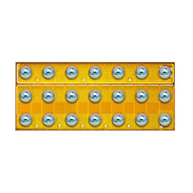
EPC2111 is listed in the FET, MOSFET Arrays range at ChipApex. The manufacturer field lists EPC. Its product description is MOSFET 2N-CH 30V 16A DIE. Review the specifications below when checking this part for your BOM.
The EPC2111 is an enhancement-mode Gallium Nitride (eGaN) power transistor configured as a half-bridge. It integrates two lateral GaN FETs, Q1 and Q2, on a single die measuring 3.5 x 1.5 mm. The device features a continuous drain-to-source voltage of 30 V and operates with a junction temperature range of –40 to 150 °C. Q1 exhibits a typical on-resistance of 19 mΩ, while Q2 demonstrates a lower typical on-resistance of 8 mΩ. Both transistors support a continuous drain current of 16 A at 25°C ambient temperature. The component is supplied in passivated die form with solder bumps, designed for high-frequency switching applications up to 10 MHz.
Verify the specific lot date code and die orientation markings upon receipt, as the component is supplied as a bare die in tape and reel format. Ensure handling procedures comply with electrostatic discharge (ESD) protocols suitable for passivated semiconductor dies. Confirm that assembly equipment supports the required 4mm pitch stencil printing and reflow profiles for SAC305 solder bumps to maintain electrical integrity.
Select this component when designing half-bridge topologies requiring operation above 1 MHz. Choose Q1 for standard switching legs where moderate on-resistance is acceptable, or Q2 for paths demanding lower conduction losses due to its reduced RDS(on). Ensure the gate drive circuit accommodates the specified 5 V logic level and negative off-state recommendation. Validate thermal management strategies against the provided junction-to-board resistance values for the target PCB copper area.
The EPC2111 belongs to the Efficient Power Conversion Corporation eGaN family of lateral gallium nitride transistors. Unlike vertical MOSFETs, these devices utilize a lateral structure that eliminates body diode reverse recovery issues. This specific model consolidates a complementary pair of switches into one die, simplifying layout and reducing loop inductance compared to discrete solutions. It represents a shift toward monolithic integration in wide-bandgap power electronics.
No official direct substitute part numbers are listed in the datasheet. When evaluating alternatives, ensure the replacement maintains the 30 V rating and compatible gate threshold characteristics. Verify that any cross-reference offers similar die dimensions for land pattern compatibility or requires significant PCB redesign. Discrete GaN FETs may require external bootstrap circuits and careful dead-time management not inherent to this integrated half-bridge.
EPC recommends using 0 V for the OFF state. Applying a negative gate drive voltage increases the reverse drain-source voltage, which may exceed safe operating limits if not carefully managed.
Q2 has a significantly lower typical on-resistance of 8 mΩ compared to Q1's 19 mΩ. This asymmetry allows designers to optimize specific legs of a converter for lower conduction losses.
No, the EPC2111 is supplied only in passivated die form with solder bumps. It requires direct mounting onto a PCB using a custom land pattern and stencil printing process.
Explore related parts through FETs, MOSFETs, Transistors, Discrete Semiconductor Products, all product categories.
 EPC2111

The activity of extra discounts on wholesale prices is in full swing…
Please fill in your contact information and we will send you the latest wholesale price list.