 ChipApex | Global Electronic Components Supplier

SEARCH
Search Product
Search Post
— IC芯片 | 连接器 | 传感器 | 被动器件 —
Search productSearch post
— IC芯片 | 连接器 | 传感器 | 被动器件 —
Consult the customer manager about the wholesale price.
consultation hotline:86-132-6715-2157
email:[email protected]
Contact the product manager for consultation. One-stop consultation is available.
Do you want a lower wholesale price? Please send us your inquiry and we will reply immediately.
FDC6327C is listed in the FET, MOSFET Arrays range at ChipApex. The manufacturer field lists onsemi. Its product description is MOSFET N/P-CH 20V 2.7A SSOT6. Review the specifications below when checking this part for your BOM.
The FDC6327C is a dual N- and P-channel MOSFET manufactured by onsemi using the PowerTrench process. It operates with a drain-source voltage of ±20 V. The N-channel device supports a continuous drain current of 2.7 A with an on-resistance of 0.08 Ω at 4.5 V gate drive, while the P-channel device handles -1.6 A with 0.17 Ω resistance under similar conditions. Total gate charge reaches 4.5 nC for the N-channel and 4.0 nC for the P-channel. Input capacitance measures 325 pF. The component functions within a junction temperature range of -55°C to +150°C and is housed in a TSOT-23-6 package.
Verify the specific ordering suffix against official documentation to confirm packaging type and tape-and-reel specifications. Ensure compliance with RoHS directives and check for any recent Product Change Notices regarding marking or assembly variations before finalizing procurement orders.
Select this component when space constraints preclude larger packages like SO-8 or TSSOP-8. Evaluate thermal resistance requirements based on the specific copper pad area used on the PCB, as junction-to-ambient resistance varies significantly with mounting surface dimensions.
This device belongs to the PowerTrench family of MOSFETs from onsemi. It serves as a high-performance solution for low-voltage switching applications where minimizing board space and power loss are critical design priorities.
Publicly confirmed substitute part numbers are not available in the provided source material.
Explore related parts through FETs, MOSFETs, Transistors, Discrete Semiconductor Products, all product categories.
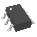 FDC6327C

The activity of extra discounts on wholesale prices is in full swing…
Please fill in your contact information and we will send you the latest wholesale price list.





