ChipApex | Global Electronic Components Supplier

SEARCH
Search Product
Search Post
— IC芯片 | 连接器 | 传感器 | 被动器件 —
Search productSearch post
— IC芯片 | 连接器 | 传感器 | 被动器件 —
Consult the customer manager about the wholesale price.
consultation hotline:86-132-6715-2157
email:[email protected]
Contact the product manager for consultation. One-stop consultation is available.
Do you want a lower wholesale price? Please send us your inquiry and we will reply immediately.
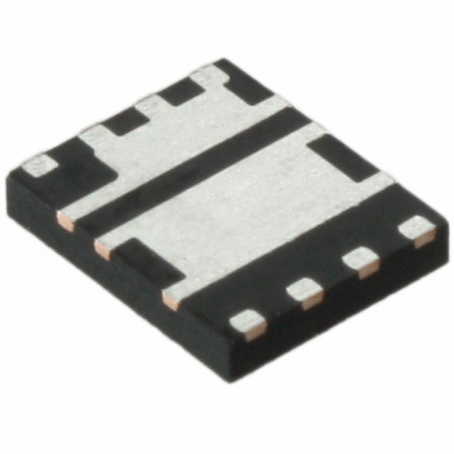
FDMS3604AS is listed in the FET, MOSFET Arrays range at ChipApex. The manufacturer field lists onsemi. Its product description is MOSFET 2N-CH 30V 13A/23A POWER56. Review the specifications below when checking this part for your BOM.
The FDMS3604AS is a PowerTrench Power Stage featuring two specialized N-Channel MOSFETs in a dual PQFN package. The switch node is internally connected to facilitate synchronous buck converter placement. Q1 (control) has max rDS(on) of 8 mΩ at VGS=10V/ID=13A and 11 mΩ at VGS=4.5V/ID=11A. Q2 (SyncFET) has max rDS(on) of 2.6 mΩ at VGS=10V/ID=23A and 3.5 mΩ at VGS=4.5V/ID=21A. Ratings include VDS of 30V, continuous ID up to 13A (Q1) and 23A (Q1), and junction temperature range of -55°C to +150°C.
Verify component authenticity through authorized distributors or direct manufacturer channels due to industry counterfeiting risks. Confirm RoHS compliance status and check current production lifecycle status, as datasheets may reference obsolete Fairchild Semiconductor branding prior to ON Semiconductor acquisition. Ensure storage conditions meet specified limits.
Select this asymmetric dual MOSFET for synchronous buck converters requiring optimized phase node performance. Verify gate drive voltage compatibility with specified rDS(on) thresholds at 10V and 4.5V. Ensure PCB layout adheres to recommended guidelines for thermal dissipation and parasitic inductance minimization to maintain stability within breakdown limits.
Originally manufactured by Fairchild Semiconductor under the PowerTrench brand, this device was acquired by ON Semiconductor. It belongs to the Power Stage family designed specifically for high-efficiency DC-DC conversion. The internal integration of control and synchronous FETs distinguishes it from discrete dual MOSFET solutions by reducing external component count and layout complexity.
FDMS3604S
It allows for easy placement and routing of synchronous buck converters while minimizing circuit inductance and reducing switch node ringing without external snubbing components.
Q1 has a max rDS(on) of 8 mΩ at VGS=10V and 11 mΩ at VGS=4.5V. Q2 has a max rDS(on) of 2.6 mΩ at VGS=10V and 3.5 mΩ at VGS=4.5V.
Yes, the SyncFET process embeds a Schottky barrier diode in parallel with the PowerTrench MOSFET, exhibiting characteristics similar to a discrete external Schottky diode.
Explore related parts through FETs, MOSFETs, Transistors, Discrete Semiconductor Products, all product categories.
 FDMS3604AS

The activity of extra discounts on wholesale prices is in full swing…
Please fill in your contact information and we will send you the latest wholesale price list.