ChipApex | Global Electronic Components Supplier

SEARCH
Search Product
Search Post
— IC芯片 | 连接器 | 传感器 | 被动器件 —
Search productSearch post
— IC芯片 | 连接器 | 传感器 | 被动器件 —
Consult the customer manager about the wholesale price.
consultation hotline:86-132-6715-2157
email:[email protected]
Contact the product manager for consultation. One-stop consultation is available.
Do you want a lower wholesale price? Please send us your inquiry and we will reply immediately.
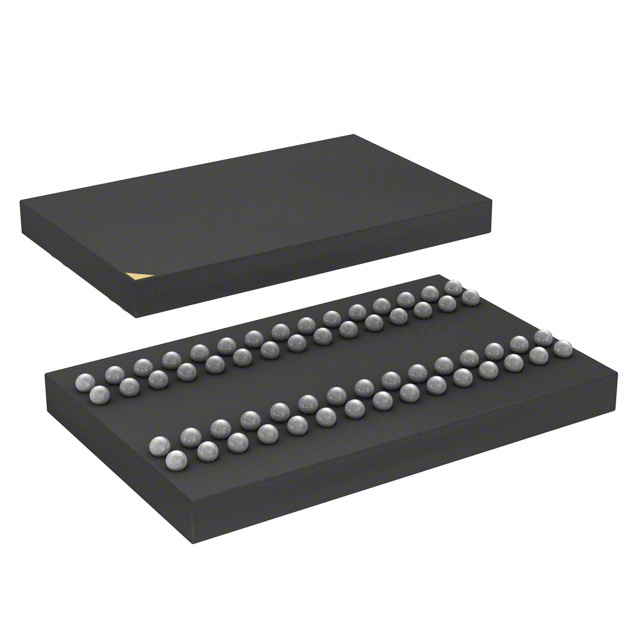
IS42S16100C1-7BLI-TR is listed in the Memory IC range at ChipApex. The manufacturer field lists ISSI, Integrated Silicon Solution Inc. Its product description is IC DRAM 16MBIT PAR 60TFBGA. Review the specifications below when checking this part for your BOM.
The IS42S16100C1 is a 16Mb Synchronous DRAM organized as 524,288 words by 16 bits across two independent banks. It operates with a single 3.3V supply and supports clock frequencies of 200, 166, and 143 MHz. The device features fully synchronous operation referenced to the positive clock edge, LV TTL interface compatibility, and programmable burst lengths including sequential and interleave sequences. It utilizes a pipeline architecture for high-speed data transfer and includes byte control via LDQM and UDQM pins.
Verify the specific speed grade suffix (e.g., -7BLI) against the required operating frequency and latency specifications. Confirm package type availability, such as 50-pin TSOP-II or 60-ball fBGA, matches the target PCB layout. Ensure the industrial temperature range variant is selected if operation below 0°C is required. Cross-reference the latest datasheet revision for any updates to absolute maximum ratings or electrical characteristics before finalizing orders.
Select this component when a 16-bit wide synchronous DRAM interface is required with dual-bank independence. Choose based on the necessary clock frequency performance tier and the preferred physical package format for the assembly process. Consider the LV TTL interface compatibility for direct connection to standard logic controllers without additional level shifting in most 3.3V environments.
This part belongs to ISSI's 16Mb Synchronous DRAM family, designed for applications demanding high-speed data throughput. It shares architectural similarities with other members of the series but is distinct in its specific organization and interface timing parameters. The device represents a solution for compact, high-density memory requirements in portable and industrial electronic devices.
Public confirmed substitute part numbers are not available in the provided documentation. Verify pinout and electrical compatibility with existing designs before considering alternative manufacturers or different density parts from the same supplier.
When the A10 pin is LOW during a precharge command, only the bank selected by A11 is precharged. If A10 is HIGH, both banks are precharged simultaneously.
The CKE pin determines entry into power-down mode; dropping it from HIGH to LOW initiates the mode when both banks are idle, suppressing internal operations to reduce power dissipation.
Burst read and write operations can be forcibly terminated using the Burst Stop command, which stops data output after the CAS latency period has elapsed for reads.
Explore related parts through Memory, Integrated Circuits (ICs), all product categories, ChipApex homepage.
 IS42S16100C1-7BLI-TR

IS42S16100C1-7BLI-TR is listed in the Memory IC range at ChipApex. The manufacturer field lists ISSI, Integrated Silicon Solution Inc. Its product description is IC…
Read More
Learn what an IMU measures, how accelerometers and gyroscopes work together, why orientation estimates drift, and what to compare.
Read More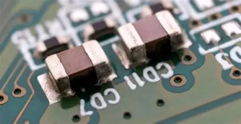
IS42S16100C1-7BLI-TR is listed in the Memory IC range at ChipApex. The manufacturer field lists ISSI, Integrated Silicon Solution Inc. Its product description is IC…
Read More
IS42S16100C1-7BLI-TR is listed in the Memory IC range at ChipApex. The manufacturer field lists ISSI, Integrated Silicon Solution Inc. Its product description is IC…
Read More
IS42S16100C1-7BLI-TR is listed in the Memory IC range at ChipApex. The manufacturer field lists ISSI, Integrated Silicon Solution Inc. Its product description is IC…
Read More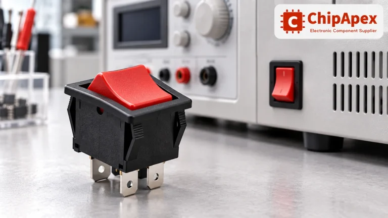
Choose a rocker switch by AC/DC ratings, contact arrangement, illumination, panel fit and sealing. Get practical checks for engineering and component sourcing.
Read More
IS42S16100C1-7BLI-TR is listed in the Memory IC range at ChipApex. The manufacturer field lists ISSI, Integrated Silicon Solution Inc. Its product description is IC…
Read More
IS42S16100C1-7BLI-TR is listed in the Memory IC range at ChipApex. The manufacturer field lists ISSI, Integrated Silicon Solution Inc. Its product description is IC…
Read More
IS42S16100C1-7BLI-TR is listed in the Memory IC range at ChipApex. The manufacturer field lists ISSI, Integrated Silicon Solution Inc. Its product description is IC…
Read More
IS42S16100C1-7BLI-TR is listed in the Memory IC range at ChipApex. The manufacturer field lists ISSI, Integrated Silicon Solution Inc. Its product description is IC…
Read More
IS42S16100C1-7BLI-TR is listed in the Memory IC range at ChipApex. The manufacturer field lists ISSI, Integrated Silicon Solution Inc. Its product description is IC…
Read More
IS42S16100C1-7BLI-TR is listed in the Memory IC range at ChipApex. The manufacturer field lists ISSI, Integrated Silicon Solution Inc. Its product description is IC…
Read More
The activity of extra discounts on wholesale prices is in full swing…
Please fill in your contact information and we will send you the latest wholesale price list.