 ChipApex | Global Electronic Components Supplier
SEARCH
Search Product
Search Post
— IC芯片 | 连接器 | 传感器 | 被动器件 —
Search productSearch post
— IC芯片 | 连接器 | 传感器 | 被动器件 —
Consult the customer manager about the wholesale price.
consultation hotline:86-132-6715-2157
email:[email protected]
Contact the product manager for consultation. One-stop consultation is available.
Do you want a lower wholesale price? Please send us your inquiry and we will reply immediately.
The J110_D26Z is an N-channel Junction Field-Effect Transistor (JFET) manufactured by onsemi. It utilizes silicon technology and is housed in a TO-92-3 Kinked Lead through-hole package. The device features a drain-source breakdown voltage of -25 V and a gate-source breakdown voltage of -35 V. Key electrical parameters include a zero-gate-voltage drain current of 5 mA, a maximum power dissipation of 625 mW, and a typical drain-source on-resistance of 50 Ohms.
Verify the specific suffix D26Z to ensure correct packaging and lead configuration compatibility with existing board layouts. Confirm RoHS compliance status via official documentation prior to integration. Cross-reference datasheet specifications against circuit requirements to validate thermal and electrical limits for the intended operating environment.
Select this component when an N-channel JFET with a -25 V rating is required for low-current analog switching. Compare its 5 mA zero-gate-voltage current against alternative models like the J112 series if higher current handling is necessary. Ensure the TO-92-3 form factor fits the mechanical constraints of the target assembly.
This part belongs to the standard discrete semiconductor product line from onsemi, focusing on general-purpose transistors. It serves as a fundamental building block for analog electronics, distinct from the manufacturer's advanced automotive or power management portfolios. The TO-92 package represents a legacy but widely used form factor for small-signal applications.
The J110_D26Z is listed as obsolete. Potential substitutes within the same family include the J111 series, though pinout and parameter differences must be verified against official datasheets before substitution.
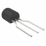 J110_D26Z
The activity of extra discounts on wholesale prices is in full swing…
Please fill in your contact information and we will send you the latest wholesale price list.





