 ChipApex | Global Electronic Components Supplier
SEARCH
Search Product
Search Post
— IC芯片 | 连接器 | 传感器 | 被动器件 —
Search productSearch post
— IC芯片 | 连接器 | 传感器 | 被动器件 —
Consult the customer manager about the wholesale price.
consultation hotline:86-132-6715-2157
email:[email protected]
Contact the product manager for consultation. One-stop consultation is available.
Do you want a lower wholesale price? Please send us your inquiry and we will reply immediately.
The onsemi J111RLRP is an N-channel depletion-mode Junction Field-Effect Transistor (JFET) designed for chopper applications. It is housed in a TO-92 package with three leads: Drain, Source, and Gate. The device supports a maximum drain-gate voltage of -35 Vdc and a gate-source voltage of -35 Vdc. Total device dissipation is rated at 350 mW at 25°C ambient temperature, derating by 2.8 mW/°C above this threshold. Operating junction temperature ranges from -65°C to +150°C. Electrical characteristics include a zero-gate-voltage drain current (IDSS) range of 2.0 mA to 20 mA and a static drain-source on resistance (rDS(on)) up to 30 Ω.
Verify the ordering suffix RLRP corresponds to the specific tape and reel packaging configuration required for automated assembly processes. Confirm that the component meets all applicable RoHS compliance standards before integration into final assemblies. Ensure proper handling procedures are followed during storage and mounting to maintain device reliability.
Select the J111RLRP when designing circuits requiring low on-resistance and high input impedance for N-channel chopper applications. Evaluate the IDSS range to ensure compatibility with the target circuit's biasing requirements. Consider the thermal derating characteristics if the application operates at elevated ambient temperatures exceeding 25°C.
The J111RLRP belongs to the J111/J112 series of JFET chopper transistors manufactured by onsemi. This series is specifically engineered for precision analog applications where low offset voltage and low drift are critical. The part utilizes standard TO-92 leaded packaging, facilitating through-hole mounting in various electronic designs.
Direct substitutes within the same family include the J111RLRA and J111RL1, which share identical electrical specifications but may differ in packaging format. Verify pinout compatibility and package dimensions when replacing components to ensure mechanical fit and correct electrical connection.
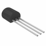 J111RLRP
The activity of extra discounts on wholesale prices is in full swing…
Please fill in your contact information and we will send you the latest wholesale price list.







