 ChipApex | Global Electronic Components Supplier
SEARCH
Search Product
Search Post
— IC芯片 | 连接器 | 传感器 | 被动器件 —
Search productSearch post
— IC芯片 | 连接器 | 传感器 | 被动器件 —
Consult the customer manager about the wholesale price.
consultation hotline:86-132-6715-2157
email:[email protected]
Contact the product manager for consultation. One-stop consultation is available.
Do you want a lower wholesale price? Please send us your inquiry and we will reply immediately.
The J310ZL1G is an N-channel depletion-mode Junction Field-Effect Transistor (JFET) designed for VHF and UHF amplifier applications. It operates with a maximum drain-source voltage of 25 Vdc and a total device dissipation of 350 mW at 25°C ambient temperature. The device features a zero-gate-voltage drain current range of 24 to 60 mA and a gate-source cutoff voltage between -2.0 V and -6.5 V. Packaged in a TO-92 outline, it supports junction temperatures from -65°C to +125°C.
Verify the specific ordering suffix ZL1G against official documentation to confirm tape and ammo box packaging containing 2000 units. Confirm Pb-free status via the G suffix if required. Ensure compatibility with TO-92 mounting requirements and validate thermal derating curves for high-temperature environments before finalizing supply agreements.
Select this component when designing circuits requiring N-channel depletion mode behavior with specific transconductance profiles. Compare the J310 parameters against the J309 variant, noting differences in zero-gate-voltage drain current and cutoff voltage ranges. Ensure the selected part meets the required operating frequency and power dissipation limits for the target application.
This device belongs to the J309/J310 series of preferred N-channel depletion JFETs manufactured by onsemi. These components are specifically engineered for radio frequency applications, offering stable performance across varying temperatures. The series provides standardized pinouts and electrical characteristics for consistent integration into RF designs.
The J309 serves as a functional alternative within the same series, sharing identical package dimensions and pinout configurations. Verify that the J309's lower drain current and cutoff voltage specifications align with the circuit requirements previously met by the J310ZL1G.
The common-source forward transconductance is typically 12 mmhos at 100 MHz under standard test conditions.
The gate reverse current is specified as -1.0 nA at 25°C and -1.0 µA at 125°C when the gate-source voltage is -15 Vdc.
The maximum junction temperature range extends up to +125°C for reliable operation.


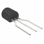 J310ZL1G
The activity of extra discounts on wholesale prices is in full swing…
Please fill in your contact information and we will send you the latest wholesale price list.




