 ChipApex | Global Electronic Components Supplier
SEARCH
Search Product
Search Post
— IC芯片 | 连接器 | 传感器 | 被动器件 —
Search productSearch post
— IC芯片 | 连接器 | 传感器 | 被动器件 —
Consult the customer manager about the wholesale price.
consultation hotline:86-132-6715-2157
email:[email protected]
Contact the product manager for consultation. One-stop consultation is available.
Do you want a lower wholesale price? Please send us your inquiry and we will reply immediately.
The JFE2140DR is a dual N-channel JFET in an 8-pin SOIC package. It provides ultra-low noise performance with input-referred voltage noise of 0.9 nV/√Hz at 1 kHz and IDS = 5 mA, or 1.1 nV/√Hz at 1 kHz and IDS = 2 mA. Current noise is 1.6 fA/√Hz at 1 kHz. The device features low gate current (max 10 pA), high transconductance (30 mS), and differential VGS matching of ±4 mV max. It withstands drain-to-source voltages up to 40 V and gate-to-source/gate-drain voltages down to –40 V. Operating temperature range is –40°C to +125°C.
Verify the 'DR' suffix corresponds to the SOIC-8 package when ordering. Confirm that the component meets specific thermal resistance requirements for your application, as junction-to-ambient values are provided for the SOIC variant. Ensure design accounts for the specified absolute maximum ratings regarding gate-to-source and drain-to-source voltages to prevent permanent damage.
Select this component for applications requiring extremely high input impedance combined with minimal noise contribution. It is suitable for battery-powered audio designs where low quiescent current is critical. Consider the integrated clamp nodes if external protection components would introduce unwanted leakage or nonlinear capacitance into the signal path.
This part belongs to Texas Instruments' Burr-Brown Audio discrete JFET family. It utilizes modern high-performance analog bipolar process technology, offering superior noise and matching characteristics compared to older discrete JFET technologies. It serves as a direct replacement for legacy matched-pair JFETs in high-fidelity audio and precision sensor interfaces.
No public confirmed substitute part numbers are available in the documentation.
It features integrated diodes connected to separate clamp nodes (VCH and VCL) that steer current away from the gate during surges, eliminating the need for external protection diodes.
Gate current increases as the drain-to-source voltage increases. For lowest gate input current operation, the datasheet recommends keeping the drain-to-source voltage below 5 V.
Yes, it can be configured as a cascoded front end to increase output impedance and buffer the input node from gate current flow associated with higher VDS voltages.
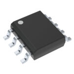 JFE2140DR
The activity of extra discounts on wholesale prices is in full swing…
Please fill in your contact information and we will send you the latest wholesale price list.





