ChipApex | Global Electronic Components Supplier

SEARCH
Search Product
Search Post
— IC芯片 | 连接器 | 传感器 | 被动器件 —
Search productSearch post
— IC芯片 | 连接器 | 传感器 | 被动器件 —
Consult the customer manager about the wholesale price.
consultation hotline:86-132-6715-2157
email:[email protected]
Contact the product manager for consultation. One-stop consultation is available.
Do you want a lower wholesale price? Please send us your inquiry and we will reply immediately.
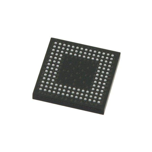
LCMXO2-640HC-5MG132I is listed in the Field Programmable Gate Array range at ChipApex. The manufacturer field lists Lattice Semiconductor Corporation. Its product description is IC FPGA 79 I/O 132CSBGA. Review the specifications below when checking this part for your BOM.
The LCMXO2-640HC-5MG132I is a Field Programmable Gate Array from the MachXO2 series by Lattice Semiconductor. It features 640 Logic Elements and 320 Adaptive Logic Modules within an 80 LAB architecture. The device provides 79 I/O pins and includes 18 kbit of embedded block RAM alongside 5 kbit of distributed RAM, totaling 47 kbit of memory resources. Operating at a maximum frequency of 388 MHz, it supports supply voltages between 2.375 V and 3.6 V with a typical operating current of 28 uA. Housed in a 132-pin CSBGA package, it functions reliably across temperatures from -40°C to +100°C.
Verify the specific speed grade suffix against official Lattice documentation to confirm timing characteristics. Ensure the component meets RoHS compliance requirements for your assembly process. Confirm that the 132-pin CSBGA footprint matches your PCB design constraints before finalizing procurement.
Select this model when requiring low static power consumption combined with moderate logic density. The 640 LE count suits simple interface bridging or protocol conversion tasks. Verify that the 79 available I/O pins meet your system connectivity needs without excessive external multiplexing.
This component belongs to the MachXO2 family, which bridges the gap between complex FPGAs and simple PLDs. It utilizes embedded flash technology to eliminate the need for external configuration memory, reducing system bill of materials and board space compared to volatile FPGA alternatives.
Direct pin-to-pin replacements within the same package are limited. Consider the LCMXO2-640ZE variant if lower voltage operation is required, though functional differences exist. Cross-series migration to MachXO3LF requires significant design adaptation due to architectural changes.
Explore related parts through Embedded, Integrated Circuits (ICs), all product categories, ChipApex homepage.
 LCMXO2-640HC-5MG132I

LCMXO2-640HC-5MG132I is listed in the Field Programmable Gate Array range at ChipApex. The manufacturer field lists Lattice Semiconductor Corporation. Its product description is IC…
Read More
LCMXO2-640HC-5MG132I is listed in the Field Programmable Gate Array range at ChipApex. The manufacturer field lists Lattice Semiconductor Corporation. Its product description is IC…
Read More
Choose logic inverter ICs by thresholds, supply, output drive and delay. Compare standard and Schmitt-trigger inputs, power sequencing and replacement checks.
Read More
Compare thermistors, RTDs, thermocouples and temperature ICs. Learn how range, accuracy, response, interfaces and mounting affect component selection.
Read More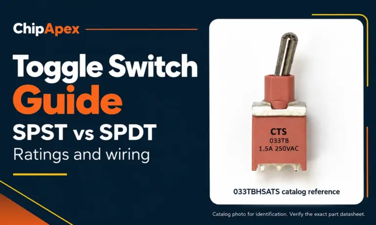
Compare SPST and SPDT toggle switches, understand AC/DC ratings, and follow wiring examples. Check contact action, mounting and parts in the ChipApex catalog.
Read More
LCMXO2-640HC-5MG132I is listed in the Field Programmable Gate Array range at ChipApex. The manufacturer field lists Lattice Semiconductor Corporation. Its product description is IC…
Read More
See how a MEMS gyroscope measures angular rate, why its angle estimate drifts, and which range, noise, interface and temperature specs to compare.
Read More
LCMXO2-640HC-5MG132I is listed in the Field Programmable Gate Array range at ChipApex. The manufacturer field lists Lattice Semiconductor Corporation. Its product description is IC…
Read More
LCMXO2-640HC-5MG132I is listed in the Field Programmable Gate Array range at ChipApex. The manufacturer field lists Lattice Semiconductor Corporation. Its product description is IC…
Read More
LCMXO2-640HC-5MG132I is listed in the Field Programmable Gate Array range at ChipApex. The manufacturer field lists Lattice Semiconductor Corporation. Its product description is IC…
Read More
LCMXO2-640HC-5MG132I is listed in the Field Programmable Gate Array range at ChipApex. The manufacturer field lists Lattice Semiconductor Corporation. Its product description is IC…
Read More
LCMXO2-640HC-5MG132I is listed in the Field Programmable Gate Array range at ChipApex. The manufacturer field lists Lattice Semiconductor Corporation. Its product description is IC…
Read More
The activity of extra discounts on wholesale prices is in full swing…
Please fill in your contact information and we will send you the latest wholesale price list.