ChipApex | Global Electronic Components Supplier

SEARCH
Search Product
Search Post
— IC芯片 | 连接器 | 传感器 | 被动器件 —
Search productSearch post
— IC芯片 | 连接器 | 传感器 | 被动器件 —
Consult the customer manager about the wholesale price.
consultation hotline:86-132-6715-2157
email:[email protected]
Contact the product manager for consultation. One-stop consultation is available.
Do you want a lower wholesale price? Please send us your inquiry and we will reply immediately.
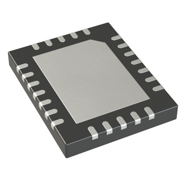
LT6372IUDC-0.2#TRPBF is listed in the Instrumentation, Op Amps, Buffer Amps range at ChipApex. The manufacturer field lists Analog Devices Inc.. Its product description is IC INST AMP 1 CIRCUIT 20QFN. Review the specifications below when checking this part for your BOM.
The LT6372IUDC-0.2#TRPBF is a precision funneling instrumentation amplifier in a 20-lead QFN package, designed for high DC accuracy and ADC interfacing. It features a gain range of 0.2 to over 200 V/V with a single external resistor. Key electrical parameters include a maximum input offset voltage of 60µV, a drift of 0.6µV/°C, and a minimum CMRR of 80dB at G=0.2. The device operates on a supply voltage from 4.75V to 35V, drawing approximately 2.75mA. It provides a 4MHz bandwidth at G=0.2, low noise density of 7nV/√Hz, and integrated output clamping and level shifting capabilities.
Verify the specific suffix #TRPBF indicates tape and reel packaging when sourcing this component. Confirm the I-grade temperature rating (-40°C to 85°C) matches your system requirements. Ensure the 20-lead QFN footprint aligns with your PCB layout constraints before finalizing procurement.
Select this part for applications requiring high precision with minimal calibration effort. The fixed G=0.2 internal setting makes it suitable for attenuating large differential signals directly into ADC ranges. Consider the H-grade variant if operation above 85°C is necessary.
This component belongs to the LT6372 family of funneling instrumentation amplifiers. It shares architectural similarities with the LT6370 but adds integrated clamping and level-shifting features. The IUDC-0.2 variant specifically utilizes the compact 3mm x 4mm QFN package for space-constrained designs.
LT6372IUDC-1#TRPBF (Different internal gain setting)
REF1 and REF2 can be used together to form a voltage divider, allowing the user to precisely level shift the amplifier's output to the center of an ADC's input range.
These pins provide integrated output clamping. The output voltage is limited to approximately 500mV beyond the voltages applied to these pins, protecting connected ADCs from overvoltage.
Explore related parts through Amplifiers, Linear, Integrated Circuits (ICs), all product categories.
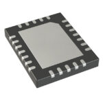 LT6372IUDC-0.2#TRPBF

LT6372IUDC-0.2#TRPBF is listed in the Instrumentation, Op Amps, Buffer Amps range at ChipApex. The manufacturer field lists Analog Devices Inc.. Its product description is…
Read More
LT6372IUDC-0.2#TRPBF is listed in the Instrumentation, Op Amps, Buffer Amps range at ChipApex. The manufacturer field lists Analog Devices Inc.. Its product description is…
Read More
LT6372IUDC-0.2#TRPBF is listed in the Instrumentation, Op Amps, Buffer Amps range at ChipApex. The manufacturer field lists Analog Devices Inc.. Its product description is…
Read More
LT6372IUDC-0.2#TRPBF is listed in the Instrumentation, Op Amps, Buffer Amps range at ChipApex. The manufacturer field lists Analog Devices Inc.. Its product description is…
Read More
LT6372IUDC-0.2#TRPBF is listed in the Instrumentation, Op Amps, Buffer Amps range at ChipApex. The manufacturer field lists Analog Devices Inc.. Its product description is…
Read More
LT6372IUDC-0.2#TRPBF is listed in the Instrumentation, Op Amps, Buffer Amps range at ChipApex. The manufacturer field lists Analog Devices Inc.. Its product description is…
Read More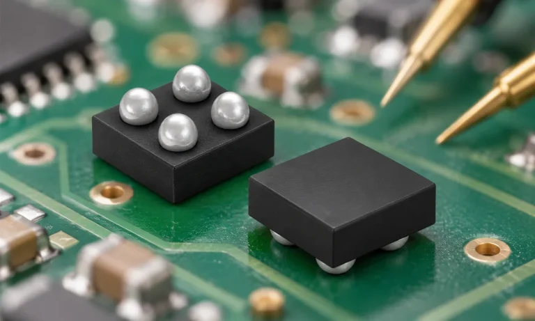
Understand how a comparator switches at a voltage threshold, why hysteresis prevents chatter, and which output and input specs matter.
Read More
LT6372IUDC-0.2#TRPBF is listed in the Instrumentation, Op Amps, Buffer Amps range at ChipApex. The manufacturer field lists Analog Devices Inc.. Its product description is…
Read More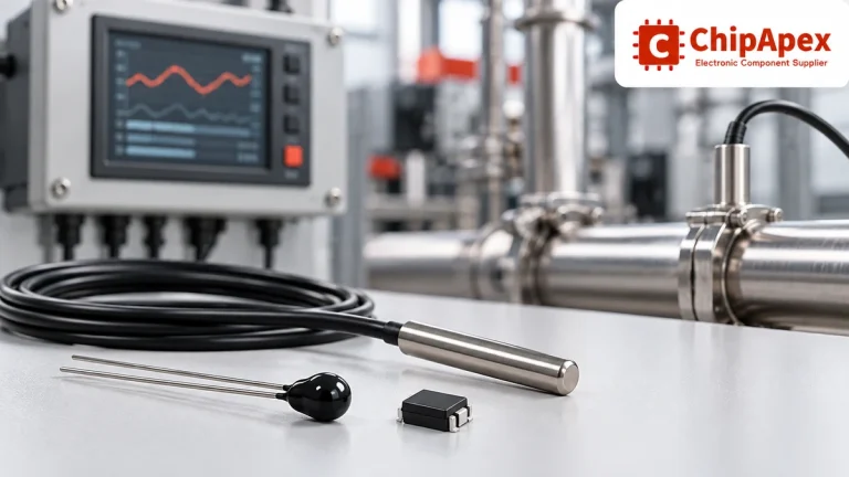
Compare thermistors, RTDs, thermocouples and temperature ICs. Learn how range, accuracy, response, interfaces and mounting affect component selection.
Read More
LT6372IUDC-0.2#TRPBF is listed in the Instrumentation, Op Amps, Buffer Amps range at ChipApex. The manufacturer field lists Analog Devices Inc.. Its product description is…
Read More
LT6372IUDC-0.2#TRPBF is listed in the Instrumentation, Op Amps, Buffer Amps range at ChipApex. The manufacturer field lists Analog Devices Inc.. Its product description is…
Read More
LT6372IUDC-0.2#TRPBF is listed in the Instrumentation, Op Amps, Buffer Amps range at ChipApex. The manufacturer field lists Analog Devices Inc.. Its product description is…
Read More
The activity of extra discounts on wholesale prices is in full swing…
Please fill in your contact information and we will send you the latest wholesale price list.