ChipApex | Global Electronic Components Supplier
SEARCH
Search Product
Search Post
— IC芯片 | 连接器 | 传感器 | 被动器件 —
Search productSearch post
— IC芯片 | 连接器 | 传感器 | 被动器件 —
Consult the customer manager about the wholesale price.
consultation hotline:86-132-6715-2157
email:[email protected]
Contact the product manager for consultation. One-stop consultation is available.
Do you want a lower wholesale price? Please send us your inquiry and we will reply immediately.
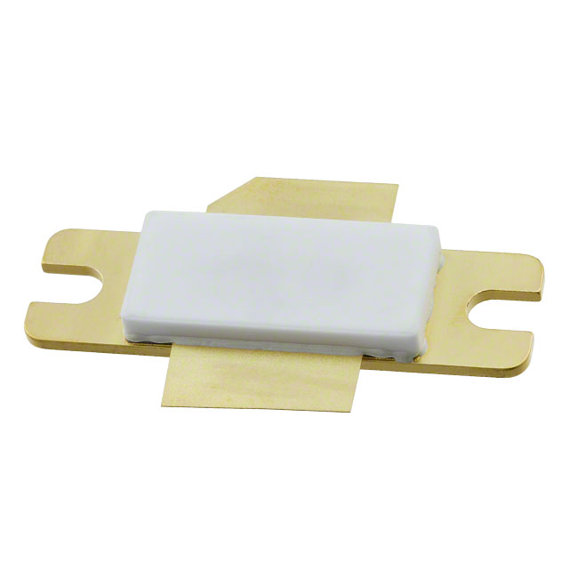
The MAGX-001090-600L00 is a depletion-mode GaN-on-SiC HEMT pulsed power transistor optimized for avionics and radar applications. It delivers 600 W peak output power across the 1030 to 1090 MHz frequency band with a 32 μs pulse width and 2% duty cycle. The device features an internally matched common-source configuration, typically operating at +50 V drain voltage. Electrical characteristics include a typical power gain of 21.4 dB and drain efficiency of 63%. Absolute maximum ratings specify a drain voltage limit of +65 V and an operating junction temperature range up to 250 °C.
Verify the specific package variant required for your application before ordering. The MAGX-001090-600L00 denotes the flanged version, while MAGX-001090-600L0S indicates the flangeless option. Confirm that the evaluation board order notes explicitly state whether it is intended for standard flange or earless flange devices to ensure compatibility with your test fixture assembly.
Select this component for high-power pulsed applications requiring operation within the 1030 to 1090 MHz band. Ensure the system can support the recommended +50 V typical drain voltage and manage thermal resistance effectively. Consider the internal matching capabilities to reduce external RF network complexity. Verify that the application environment stays within the specified -40 to +95 °C operating temperature range.
This part belongs to MACOM's MAGX series of Gallium Nitride on Silicon Carbide RF power transistors. These devices are engineered for high performance, offering high gain, efficiency, and bandwidth. The series targets demanding avionics and radar needs, leveraging advanced wafer fabrication processes to achieve superior ruggedness compared to older semiconductor technologies.
Consult MACOM directly for cross-reference data. The datasheet does not list specific substitute part numbers from other manufacturers. Any replacement must match the 1030-1090 MHz frequency range, 600 W peak power capability, and depletion-mode operational characteristics.
First set VGS to pinch-off (VP), typically -5 V. Next, turn on VDS to the nominal voltage of 50 V. Then increase VGS until the desired IDS current is reached, and finally apply the RF power to the desired level.
The absolute maximum input power limit is defined as the nominal drive power required to achieve 600 W POUT plus 3 dB.
The device has a Charged Device Model (CDM) rating of 1300 V and a Human Body Model (HBM) rating of 4000 V.
 MAGX-001090-600L00
The activity of extra discounts on wholesale prices is in full swing…
Please fill in your contact information and we will send you the latest wholesale price list.