ChipApex | Global Electronic Components Supplier
SEARCH
Search Product
Search Post
— IC芯片 | 连接器 | 传感器 | 被动器件 —
Search productSearch post
— IC芯片 | 连接器 | 传感器 | 被动器件 —
Consult the customer manager about the wholesale price.
consultation hotline:86-132-6715-2157
email:[email protected]
Contact the product manager for consultation. One-stop consultation is available.
Do you want a lower wholesale price? Please send us your inquiry and we will reply immediately.
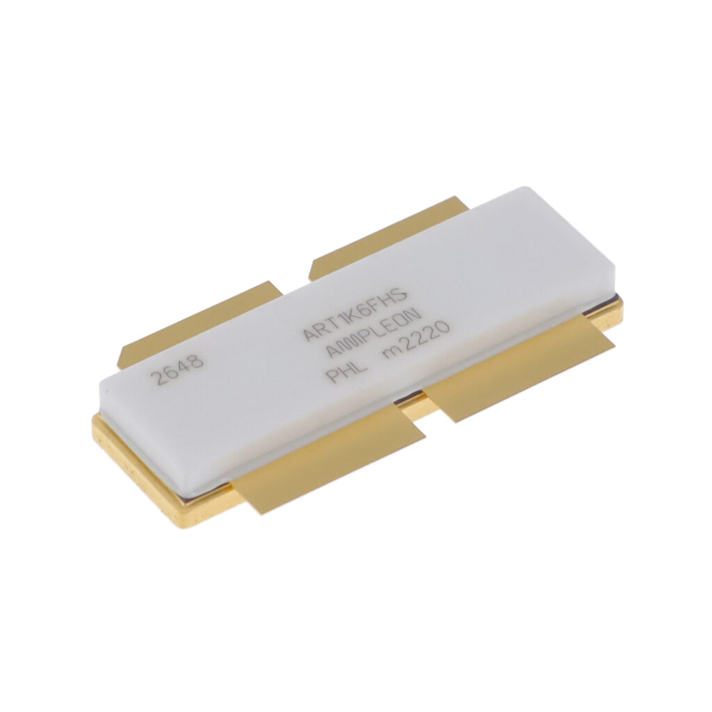
The MAGX-001214-500L00 is a gold-metalized Gallium Nitride (GaN) on Silicon Carbide (SiC) RF power transistor optimized for pulsed L-Band radar applications. It delivers 500 W peak output power within the 1200-1400 MHz frequency range using a 300 μs pulse width and 10% duty cycle at VDD = 50 V. The device features internally matched broadband Class AB operation with typical drain efficiency of 56% and power gain of 19.2 dB. It supports extended pulse conditions up to 1.0 ms at reduced voltage.
Verify the specific package variant required for the design; the MAGX-001214-500L00 denotes the flanged configuration, while MAGX-001214-500L0S indicates the flangeless version. Confirm that the application environment adheres to the specified absolute maximum ratings, particularly regarding junction temperature limits and correct device sequencing during power-up and power-down cycles to ensure long-term operational integrity.
Select this component for designs requiring high peak power density in the L-Band spectrum. Ensure the thermal management system can maintain the junction temperature below 200°C to preserve the rated MTTF. Verify that the drive circuitry can supply the necessary input power levels and that the bias sequencing follows the manufacturer's recommended protocol to prevent device damage during transient states.
This part belongs to M/A-COM Technology Solutions' portfolio of GaN on SiC RF power transistors. It is designed to replace older semiconductor technologies by offering superior bandwidth, efficiency, and load mismatch tolerance. The product line targets demanding pulsed applications where high power output and reliability are critical performance metrics.
The datasheet lists MAGX-001214-500L0S as the flangeless alternative to the MAGX-001214-500L00 flanged version. No other direct substitute part numbers are documented in the provided source material.
First set VGS to the pinch-off voltage (typically -5 V), then turn on VDS to the nominal voltage (50 V). Next, increase VGS until the desired IDS current is reached, and finally apply the RF power to the desired level.
The transistor exhibits high ruggedness and stable operation under extreme mismatch loads. It maintains stability with a VSWR-S of 3:1 and demonstrates tolerance up to a VSWR-T of 5:1 at 500 W peak output power.
Under extended pulse conditions of 1.0 ms pulse width and 10% duty cycle at VDD = 42 V, the device typically delivers 375 W peak output power with 18.5 dB power gain and 55% drain efficiency.



 MAGX-001214-500L00
The activity of extra discounts on wholesale prices is in full swing…
Please fill in your contact information and we will send you the latest wholesale price list.