ChipApex | Global Electronic Components Supplier

SEARCH
Search Product
Search Post
— IC芯片 | 连接器 | 传感器 | 被动器件 —
Search productSearch post
— IC芯片 | 连接器 | 传感器 | 被动器件 —
Consult the customer manager about the wholesale price.
consultation hotline:86-132-6715-2157
email:[email protected]
Contact the product manager for consultation. One-stop consultation is available.
Do you want a lower wholesale price? Please send us your inquiry and we will reply immediately.
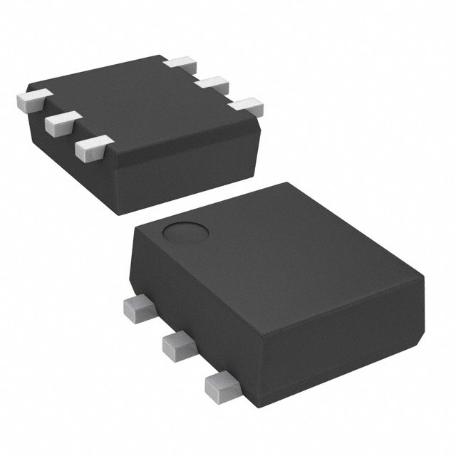
MCH6601-TL-E is listed in the FET, MOSFET Arrays range at ChipApex. The manufacturer field lists onsemi. Its product description is MOSFET 2P-CH 30V 0.2A 6MCPH. Review the specifications below when checking this part for your BOM.
The MCH6601-TL-E is a dual P-Channel Power MOSFET from onsemi, housed in an MCPH6 package. It features a drain-to-source voltage of -30V and a continuous DC drain current of -0.2A. The device exhibits low ON-resistance, with typical values of 10.4Ω at VGS=-4V and 54Ω at VGS=-1.5V. Switching performance includes a turn-on delay of 24ns and a fall time of 130ns. Total gate charge is typically 1.43nC. The component supports a junction temperature up to 150°C and allows for 1.5V drive operation.
Verify the specific ordering suffix TL-E corresponds to the tape and reel packaging format containing 3,000 pieces per reel. Confirm that the MCPH6 package dimensions align with the target land pattern design. Ensure handling procedures account for the specified ESD immunity characteristics during assembly processes.
Select this component when a dual P-channel configuration is required in a minimal footprint. Evaluate the RDS(on) specifications against the intended load current and gate drive voltage levels. Consider the thermal dissipation limits relative to the PCB substrate area available for heat spreading.
This part belongs to the MCH6601 series of dual power MOSFETs manufactured by onsemi. It utilizes the MCPH6 package, which is equivalent to JEITA/JEDEC standards SC-88, SC-70-6, and SOT-363. The device is designed for applications prioritizing space efficiency and switching speed.
Direct substitutes must match the dual P-channel topology, -30V rating, and MCPH6/SOT-363 package. Verify electrical parameters such as RDS(on) and switching times against the original datasheet requirements before implementation.
The allowable power dissipation is 0.8W when mounted on a ceramic substrate measuring 900mm² x 0.8mm.
Pin 1 is Source1, Pin 2 is Gate1, Pin 3 is Drain2, Pin 4 is Source2, Pin 5 is Gate2, and Pin 6 is Drain1.
The typical forward transfer admittance (|yfs|) is 110 mS at VDS=-10V and ID=-50mA.
Explore related parts through FETs, MOSFETs, Transistors, Discrete Semiconductor Products, all product categories.
 MCH6601-TL-E

The activity of extra discounts on wholesale prices is in full swing…
Please fill in your contact information and we will send you the latest wholesale price list.