 ChipApex | Global Electronic Components Supplier
SEARCH
Search Product
Search Post
— IC芯片 | 连接器 | 传感器 | 被动器件 —
Search productSearch post
— IC芯片 | 连接器 | 传感器 | 被动器件 —
Consult the customer manager about the wholesale price.
consultation hotline:86-132-6715-2157
email:[email protected]
Contact the product manager for consultation. One-stop consultation is available.
Do you want a lower wholesale price? Please send us your inquiry and we will reply immediately.
The MRF18085ALSR3 is an N-channel enhancement-mode lateral MOSFET designed for GSM and GSM EDGE base station applications within the 1805–1880 MHz frequency band. It operates at a drain-source voltage of 26 Vdc, delivering 85 Watts CW output power with typical gain of 15 dB and efficiency of 52%. The device features internal matching, integrated ESD protection, and high thermal stability. It is housed in a CASE 465A-06 package (NI-780S) and supplied in tape and reel format.
Verify the specific ordering suffix 'SR3' to confirm the component is supplied in tape and reel packaging containing 250 units per 56 mm reel. Ensure the lead frame plating specification matches the 'L' suffix requirement for nominal 40μm gold thickness. Confirm compliance with RoHS standards during procurement validation.
Select this component for designs requiring high gain and efficiency in the 1805–1880 MHz range. The internal matching simplifies impedance network design. Verify that the application supports the specified 26 Vdc operating voltage and 800 mA quiescent current. Ensure the PCB layout accommodates the CASE 465A-06 package dimensions and thermal requirements.
This part belongs to the Freescale Semiconductor RF Power Field Effect Transistors family, specifically lateral N-channel enhancement-mode MOSFETs. It is archived under document number MRF18085A Rev. 6. The 'SR3' suffix denotes the specific packaging configuration, distinguishing it from the standard 'LR3' variant which uses a different case style.
The MRF18085ALR3 is a related variant within the same datasheet but utilizes the CASE 465-06 package instead of the CASE 465A-06 package used by the MRF18085ALSR3. Verify mechanical fit and pinout compatibility before substitution.
The maximum drain-source voltage (VDSS) rating is -0.5 to +65 Vdc.
No, the device is internally matched on both input and output for ease of use.
The typical power gain is 15 dB at 85 Watts CW output power.
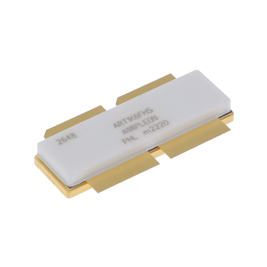


 MRF18085ALSR3
The activity of extra discounts on wholesale prices is in full swing…
Please fill in your contact information and we will send you the latest wholesale price list.




