ChipApex | Global Electronic Components Supplier
SEARCH
Search Product
Search Post
— IC芯片 | 连接器 | 传感器 | 被动器件 —
Search productSearch post
— IC芯片 | 连接器 | 传感器 | 被动器件 —
Consult the customer manager about the wholesale price.
consultation hotline:86-132-6715-2157
email:[email protected]
Contact the product manager for consultation. One-stop consultation is available.
Do you want a lower wholesale price? Please send us your inquiry and we will reply immediately.
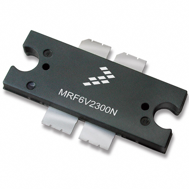
The MRF5S9100NBR1 is an N-channel enhancement-mode lateral MOSFET designed for broadband commercial and industrial applications up to 1000 MHz. It operates at a drain-source voltage of 26 Vdc with a maximum rating of 68 Vdc. The device delivers 20 Watts average output power at 880 MHz, achieving a typical power gain of 19.5 dB and a drain efficiency of 28%. It features internal input matching and integrated ESD protection.
Verify the part number against official manufacturer documentation to confirm lead-free termination status indicated by the suffix. Ensure compatibility with existing thermal management solutions, as the device supports junction temperatures up to 200°C. Confirm that the procurement channel provides valid traceability for this specific Freescale/NXP component.
Select this component for designs requiring high gain and broadband capability within the sub-1000 MHz range. It is optimized for 26V base station environments where internal matching reduces external component count. Consider the TO-270 or TO-272 package options based on board space constraints and thermal requirements.
This device belongs to the MRF5S series of RF power field effect transistors manufactured by Freescale Semiconductor, now NXP USA Inc. The product line targets high-performance RF amplification needs in commercial and industrial sectors, emphasizing ruggedness and wideband utility.
The MRF5S9100NBR1 replaces the MRF5S9100MR1 and MRF5S9100MBR1. There are no form, fit, or function changes associated with this replacement. The 'N' suffix indicates a transition to lead-free terminations.
The maximum drain-source voltage (VDSS) rating is +68 Vdc.
Yes, the device is internally matched for ease of use in amplifier designs.
The maximum operating junction temperature (TJ) is 200°C.
 MRF5S9100NBR1
The activity of extra discounts on wholesale prices is in full swing…
Please fill in your contact information and we will send you the latest wholesale price list.