 ChipApex | Global Electronic Components Supplier
SEARCH
Search Product
Search Post
— IC芯片 | 连接器 | 传感器 | 被动器件 —
Search productSearch post
— IC芯片 | 连接器 | 传感器 | 被动器件 —
Consult the customer manager about the wholesale price.
consultation hotline:86-132-6715-2157
email:[email protected]
Contact the product manager for consultation. One-stop consultation is available.
Do you want a lower wholesale price? Please send us your inquiry and we will reply immediately.
The MRF6S9045NR1 is an N-Channel Enhancement-Mode Lateral MOSFET designed for broadband commercial and industrial applications up to 1000 MHz. It operates at a drain-source voltage of 68 Vdc with a typical power gain of 22.7 dB at 880 MHz. The device delivers 10 Watts average output power in single-carrier N-CDMA configurations and supports 45 Watts CW output power within the 921-960 MHz band. It features integrated ESD protection, lead-free terminations, and a junction temperature capability of 225°C.
Verify component authenticity through authorized distributors or direct manufacturer channels. Confirm that the specific ordering suffix matches the required package type, as the R1 suffix indicates tape and reel packaging. Ensure compliance with environmental regulations by checking for lead-free termination markings on the physical device. Validate all electrical parameters against the official datasheet before integration into final designs.
Select this component for high-power broadband applications requiring stable performance across wide frequency ranges. Consider the 28 Vdc operating voltage and the requirement for robust thermal management due to the 225°C junction capability. Evaluate impedance matching networks based on the provided series equivalent large-signal impedance parameters. Ensure the design accommodates the TO-270-2 or TO-272-2 surface mount packages.
This device belongs to the Freescale Semiconductor RF Power Field Effect Transistor family, specifically designed for LDMOS technology. It serves as a broadband solution for commercial and industrial radio frequency applications. The product line emphasizes high gain and ruggedness, making it suitable for demanding base station environments where reliability and thermal performance are critical.
The MRF6S9045NR1 has been replaced by the MRFE6S9045NR1. Refer to Device Migration PCN12895 for detailed transition information. The variant MRF6S9045NBR1 is no longer manufactured.
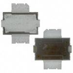 MRF6S9045NR1
The activity of extra discounts on wholesale prices is in full swing…
Please fill in your contact information and we will send you the latest wholesale price list.





