ChipApex | Global Electronic Components Supplier
SEARCH
Search Product
Search Post
— IC芯片 | 连接器 | 传感器 | 被动器件 —
Search productSearch post
— IC芯片 | 连接器 | 传感器 | 被动器件 —
Consult the customer manager about the wholesale price.
consultation hotline:86-132-6715-2157
email:[email protected]
Contact the product manager for consultation. One-stop consultation is available.
Do you want a lower wholesale price? Please send us your inquiry and we will reply immediately.
The MRF6S9060MR1 is an N-Channel Enhancement-Mode Lateral MOSFET designed for broadband commercial and industrial applications up to 1000 MHz. It operates at a drain-source voltage of 68 Vdc and supports junction temperatures up to 225°C. The device delivers 60 Watts CW output power with 20 dB gain and 63% efficiency in GSM bands (921-960 MHz). In single-carrier N-CDMA at 880 MHz, it provides 14 Watts average output with 21.4 dB gain and 32.1% efficiency.
Verify the specific suffix configuration against the datasheet to ensure correct packaging and termination specifications. Confirm RoHS compliance status as indicated by the 'N' suffix. Check current manufacturing availability, as related variants may have undergone obsolescence or migration notifications. Validate that the procurement channel sources directly from authorized distributors to guarantee component authenticity and traceability.
Select this component for designs requiring high thermal stability and broadband operation within the 850 to 960 MHz range. Ensure the application utilizes a 28-volt supply rail to match the specified operating conditions. Verify that the system can accommodate the required gate threshold voltage and quiescent current levels. Consider the TO-270 or TO-272 package options based on available board space and mounting constraints.
This lateral N-channel MOSFET belongs to the Freescale Semiconductor RF power transistor family, now part of NXP Semiconductors. It is engineered specifically for demanding wireless communication infrastructure where linearity and power density are critical. The device represents a mature technology platform optimized for cost-effective deployment in cellular base stations.
Refer to Device Migration notification PCN12895 regarding the transition from MRF6S9060NR1 to MRFE6S9060NR1. The MRF6S9060NBR1 variant is no longer manufactured. Consult official documentation for pinout compatibility and electrical equivalence before substituting.
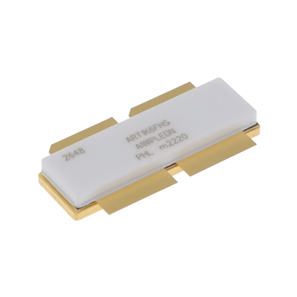


 MRF6S9060MR1
The activity of extra discounts on wholesale prices is in full swing…
Please fill in your contact information and we will send you the latest wholesale price list.