 ChipApex | Global Electronic Components Supplier
SEARCH
Search Product
Search Post
— IC芯片 | 连接器 | 传感器 | 被动器件 —
Search productSearch post
— IC芯片 | 连接器 | 传感器 | 被动器件 —
Consult the customer manager about the wholesale price.
consultation hotline:86-132-6715-2157
email:[email protected]
Contact the product manager for consultation. One-stop consultation is available.
Do you want a lower wholesale price? Please send us your inquiry and we will reply immediately.
The MRF7S18125BHSR3 is an N-channel enhancement-mode lateral MOSFET designed for GSM and GSM EDGE base station applications operating between 1800 MHz and 2000 MHz. It supports Class AB and Class C modulation in cellular environments. The device delivers a typical CW output power of 125 Watts at 1930 MHz with a drain efficiency of 55% under 28 Volts. For GSM EDGE, it provides 57 Watts average power with 39% efficiency and 2.6% rms EVM. It features internal matching, integrated ESD protection, and RoHS compliance.
Verify the specific ordering suffix against official documentation to confirm packaging details. Confirm that the component meets current environmental standards such as RoHS compliance. Ensure the supplier provides valid traceability documents. Validate the part number against the manufacturer's latest datasheet revision history to avoid obsolete or discontinued variants.
Select this component for high-power RF applications requiring internal matching to reduce external passive components. Consider its thermal characteristics and junction temperature limits when designing heat dissipation systems. Evaluate its performance across the specified frequency band to ensure compatibility with target modulation schemes like GSM EDGE.
This device belongs to the MRF7S18125BH family of RF power lateral MOSFETs from Freescale Semiconductor, now NXP Semiconductors. These transistors are engineered specifically for demanding wireless infrastructure environments. The SR3 suffix indicates tape and reel packaging configuration.
MRF7S18125BHR3
The maximum operating voltage (VDD) is rated at 32 Vdc.
No, the device is internally matched on both the input and output sides for ease of use.
The typical EVM is 2.6% rms during GSM EDGE application testing.
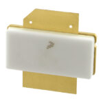 MRF7S18125BHSR3
The activity of extra discounts on wholesale prices is in full swing…
Please fill in your contact information and we will send you the latest wholesale price list.





