ChipApex | Global Electronic Components Supplier
SEARCH
Search Product
Search Post
— IC芯片 | 连接器 | 传感器 | 被动器件 —
Search productSearch post
— IC芯片 | 连接器 | 传感器 | 被动器件 —
Consult the customer manager about the wholesale price.
consultation hotline:86-132-6715-2157
email:[email protected]
Contact the product manager for consultation. One-stop consultation is available.
Do you want a lower wholesale price? Please send us your inquiry and we will reply immediately.
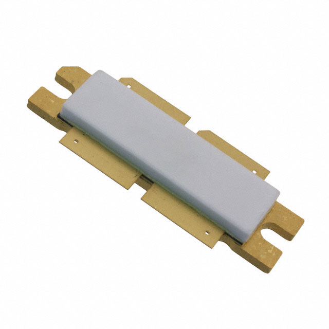
The MRF8S21200HR6 is an N-Channel Enhancement-Mode Lateral MOSFET designed for W-CDMA and LTE base station applications operating between 2110 MHz and 2170 MHz. It supports Class AB and Class C modulation formats with a drain-source voltage of 65 Vdc and an operating voltage of 32 Vdc. Typical single-carrier W-CDMA performance at 2140 MHz yields 48 Watts average output power, 18.1 dB gain, and 32.6% drain efficiency under 28 Volts and 1400 mA quiescent current conditions.
Verify the specific suffix configuration against the official datasheet before procurement. The R6 suffix indicates a tape and reel packaging format containing 150 units on a 56 mm reel. Confirm that the component status aligns with current manufacturing availability as product lifecycles may change without notice.
Select this device for wideband cellular infrastructure requiring high linearity and ruggedness. Ensure the thermal management system can handle the junction-to-case thermal resistance characteristics. Validate impedance matching networks using the provided series equivalent large-signal impedance parameters for optimal broadband performance across the specified frequency range.
This lateral N-channel RF power MOSFET belongs to the MRF8S family developed by Freescale Semiconductor. It utilizes a Case 375D-05 package style (NI-1230) designed for surface mount applications in high-power radio frequency environments. The technology focuses on providing robust performance for modern digital cellular communication standards.
Consult official manufacturer documentation for verified substitute part numbers. Cross-referencing requires matching electrical specifications, package dimensions, and thermal characteristics to ensure functional compatibility in existing designs.
The maximum drain-source voltage rating is +65 Vdc.
Yes, the MRF8S21200HR6 features internally matched input and output networks for ease of use.
The typical power gain at 2140 MHz is 18.1 dB under standard test conditions.
 MRF8S21200HR6
The activity of extra discounts on wholesale prices is in full swing…
Please fill in your contact information and we will send you the latest wholesale price list.