 ChipApex | Global Electronic Components Supplier
SEARCH
Search Product
Search Post
— IC芯片 | 连接器 | 传感器 | 被动器件 —
Search productSearch post
— IC芯片 | 连接器 | 传感器 | 被动器件 —
Consult the customer manager about the wholesale price.
consultation hotline:86-132-6715-2157
email:[email protected]
Contact the product manager for consultation. One-stop consultation is available.
Do you want a lower wholesale price? Please send us your inquiry and we will reply immediately.
The MRFE6VP5150NR1 is a high ruggedness N-channel enhancement-mode lateral MOSFET designed for wideband RF power applications. It operates across a frequency range of 1.8 to 600 MHz with a drain-source voltage rating of 133 Vdc and a maximum total device dissipation of 952 W at 25°C case temperature. The transistor delivers 150 W CW output power at 230 MHz and up to 179 W in the 87.5–108 MHz band, both at 50 Vdc. It features unmatched input and output designs, integrated stability enhancements, and ESD protection circuitry.
Verify component authenticity through authorized channels as the MRFE6VP5150N series is listed as End of Life. Confirm package integrity and moisture sensitivity level (MSL 3) prior to soldering. Ensure compliance with EU RoHS standards and check for REACH SVHC presence. Validate that the R1 suffix corresponds to the specified tape and reel packaging configuration.
Select this component for designs requiring high power density and broadband operation between 1.8 and 600 MHz. Consider the TO-270WB-4 plastic package for thermal management capabilities. Evaluate the need for external biasing circuits to maintain optimal quiescent current. Assess system requirements against the 133 Vdc drain-source voltage limit and junction temperature constraints.
This device belongs to the Freescale Semiconductor RF Power LDMOS Transistors family, specifically engineered for high ruggedness. It serves as an N-channel enhancement-mode lateral MOSFET suitable for demanding RF environments. The product line emphasizes performance in wideband applications where reliability under mismatched load conditions is critical.
Public confirmed substitute part numbers are not available in the provided documentation.
The maximum drain-source voltage (VDSS) rating is -0.5 to +133 Vdc.
The device exhibits extreme ruggedness, showing no degradation when subjected to VSWR greater than 65:1 at all phase angles with 3 dB overdrive.
The device supports Human Body Model testing up to 2500 V, Machine Model testing up to 250 V, and Charge Device Model testing up to 1200 V.
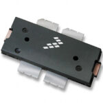 MRFE6VP5150NR1
The activity of extra discounts on wholesale prices is in full swing…
Please fill in your contact information and we will send you the latest wholesale price list.





