ChipApex | Global Electronic Components Supplier
SEARCH
Search Product
Search Post
— IC芯片 | 连接器 | 传感器 | 被动器件 —
Search productSearch post
— IC芯片 | 连接器 | 传感器 | 被动器件 —
Consult the customer manager about the wholesale price.
consultation hotline:86-132-6715-2157
email:[email protected]
Contact the product manager for consultation. One-stop consultation is available.
Do you want a lower wholesale price? Please send us your inquiry and we will reply immediately.
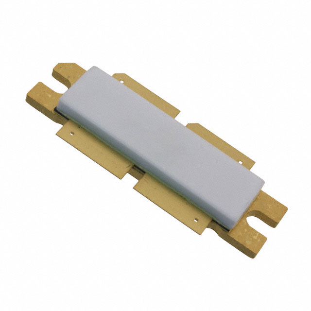
The MRFE6VP61K25HR6 is a high ruggedness N-channel enhancement-mode lateral MOSFET designed for wide frequency range utilization between 1.8 and 600 MHz. It operates with a maximum drain-source voltage of 50 Vdc and delivers up to 1250 W continuous wave output power at 230 MHz. The device features unmatched input and output designs, allowing flexible single-ended or push-pull configurations. It includes integrated ESD protection suitable for linear applications and Class C operation.
Verify the specific suffix HR6 against official documentation to confirm packaging details. The R6 suffix indicates tape and reel delivery containing 150 units on a 56 mm width, 13-inch reel. Confirm current manufacturing status and availability through authorized NXP distributors, as product lifecycles may change without notice.
Select this component for wideband RF power amplification requiring high ruggedness and significant output power within the sub-ghz to vhf bands. Ensure thermal management supports the specified junction temperature limits. Validate impedance matching networks using the provided series equivalent large-signal impedance parameters for optimal performance in both single-ended and balanced configurations.
This part belongs to the MRFE6VP61K25H family of wideband RF power LDMOS transistors. It shares core electrical characteristics with variants like the MRFE6VP61K25HR5 and MRFE6VP61K25HSR5, differing primarily in package type and shipping configuration. The family is characterized by its ability to handle extreme load mismatches while maintaining stable operation under high voltage conditions.
MRFE6VP61K25HR5
The maximum operating junction temperature is 225 °C.
Yes, the device can be used in either single-ended or push-pull configurations due to its unmatched input and output designs.
The typical drain efficiency is 74.6% when operating at 230 MHz with 1250 W CW output power and a 50 V supply.
 MRFE6VP61K25HR6
The activity of extra discounts on wholesale prices is in full swing…
Please fill in your contact information and we will send you the latest wholesale price list.