ChipApex | Global Electronic Components Supplier
SEARCH
Search Product
Search Post
— IC芯片 | 连接器 | 传感器 | 被动器件 —
Search productSearch post
— IC芯片 | 连接器 | 传感器 | 被动器件 —
Consult the customer manager about the wholesale price.
consultation hotline:86-132-6715-2157
email:[email protected]
Contact the product manager for consultation. One-stop consultation is available.
Do you want a lower wholesale price? Please send us your inquiry and we will reply immediately.
The MRFE6VS25LR5 is an N-channel enhancement-mode lateral MOSFET RF power transistor designed for ISM, broadcast, and aerospace applications. It operates from 1.8 to 2000 MHz with a drain-source voltage of 133 Vdc and delivers 25 W output power at 50 Vdc. The device features extreme ruggedness, supporting VSWRs exceeding 65:1 without degradation. It utilizes the NI-360H-2L package and includes integrated stability enhancements and extended ESD protection.
Verify the R5 suffix indicates a 50-unit reel quantity on a 32 mm tape width. Confirm the NI-360H-2L package type matches design requirements. Ensure compatibility with the specified thermal management solutions for the junction-to-case resistance values provided in the datasheet.
Select this component for designs requiring broad bandwidth and high load mismatch tolerance. Consider the 1.4 °C/W thermal resistance for heat sink sizing. Verify gate threshold voltage ranges align with biasing circuits. Evaluate the MTTF calculator data against operational temperature constraints.
This part belongs to the MRFE6VS25L family of wideband RF power LDMOS transistors. It shares core electrical characteristics with the MRFE6VS25N variant but differs in packaging and delivery format. The device represents NXP's enhanced ruggedness platform technology for high-power RF amplification.
MRFE6VS25N
The maximum drain-source voltage (VDSS) is rated at -0.5 to +133 Vdc.
The transistor exhibits extreme ruggedness, showing no device degradation when subjected to VSWRs greater than 65:1 at all phase angles with up to 3 dB overdrive.
The device passes 2000 V for the Human Body Model, 200 V for the Machine Model, and 1200 V for the Charge Device Model.

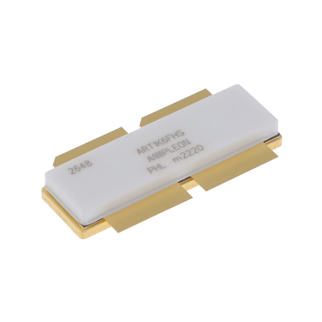

 MRFE6VS25LR5
The activity of extra discounts on wholesale prices is in full swing…
Please fill in your contact information and we will send you the latest wholesale price list.