 ChipApex | Global Electronic Components Supplier

SEARCH
Search Product
Search Post
— IC芯片 | 连接器 | 传感器 | 被动器件 —
Search productSearch post
— IC芯片 | 连接器 | 传感器 | 被动器件 —
Consult the customer manager about the wholesale price.
consultation hotline:86-132-6715-2157
email:[email protected]
Contact the product manager for consultation. One-stop consultation is available.
Do you want a lower wholesale price? Please send us your inquiry and we will reply immediately.
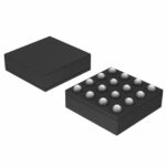
NBSG11BAR2 is listed in the Clock Buffers, Drivers range at ChipApex. The manufacturer field lists onsemi. Its product description is IC CLK BUFFER 1:2 12GHZ 16FCBGA. Review the specifications below when checking this part for your BOM.
The NBSG11BAR2 is a 2.5V/3.3V SiGe differential clock driver with RSECL outputs, manufactured by onsemi. It functions as a 1-to-2 fanout buffer optimized for low skew and ultra-low jitter. The device accepts NECL, PECL, CML, LVCMOS, LVTTL, or LVDS inputs via internal 50Ω termination resistors. Outputs provide a 400 mV peak-to-peak RSECL swing. Maximum input frequency reaches 12 GHz typical, with propagation delay at 125 ps typical. It operates within VCC ranges of 2.375 V to 3.465 V (VEE = 0 V) or VEE ranges of -2.375 V to -3.465 V (VCC = 0 V).
Verify the BA suffix indicates FCBGA-16 packaging in tape and reel format. Confirm RoHS compliance status if required for specific manufacturing processes. Ensure thermal management meets junction-to-ambient resistance requirements for the selected airflow conditions.
Select based on required operating temperature range; QFN packages support up to 85°C while FCBGA/FCLGA are rated to 70°C. Verify interface compatibility with source logic levels such as LVDS or PECL. Check power supply configuration to determine appropriate VCC or VEE biasing scheme.
This component belongs to the NBSG11 series of differential clock drivers. The BAR2 suffix specifically denotes the FCBGA-16 package variant supplied in tape and reel quantities of 100 units per tray. It replaces older discrete buffer solutions in high-frequency applications.
Public confirmed substitute part numbers are not available in the provided documentation. Evaluate alternative models from the same family, such as NBSG11MNG or NBSG11BA, ensuring package and electrical specifications match the design requirements.
The typical propagation delay is 125 ps, with a maximum guaranteed value of 160 ps across the operating temperature range.
An external voltage should be applied to the unused complementary input. The nominal voltage is VCC/2 for LVCMOS inputs.
The device provides a Reduced Swing ECL (RSECL) output with a peak-to-peak amplitude of 400 mV typical, ranging from 350 mV to 525 mV depending on conditions.
Explore related parts through Clock/Timing, Integrated Circuits (ICs), all product categories, ChipApex homepage.
 NBSG11BAR2
NBSG11BAR2 is listed in the Clock Buffers, Drivers range at ChipApex. The manufacturer field lists onsemi. Its product description is IC CLK BUFFER 1:2…
Read More
NBSG11BAR2 is listed in the Clock Buffers, Drivers range at ChipApex. The manufacturer field lists onsemi. Its product description is IC CLK BUFFER 1:2…
Read More
NBSG11BAR2 is listed in the Clock Buffers, Drivers range at ChipApex. The manufacturer field lists onsemi. Its product description is IC CLK BUFFER 1:2…
Read More
NBSG11BAR2 is listed in the Clock Buffers, Drivers range at ChipApex. The manufacturer field lists onsemi. Its product description is IC CLK BUFFER 1:2…
Read More
NBSG11BAR2 is listed in the Clock Buffers, Drivers range at ChipApex. The manufacturer field lists onsemi. Its product description is IC CLK BUFFER 1:2…
Read More
Understand RF attenuator dB values, fixed and programmable types, impedance, power limits and noise tradeoffs before choosing parts for an RF signal path.
Read More
NBSG11BAR2 is listed in the Clock Buffers, Drivers range at ChipApex. The manufacturer field lists onsemi. Its product description is IC CLK BUFFER 1:2…
Read More
NBSG11BAR2 is listed in the Clock Buffers, Drivers range at ChipApex. The manufacturer field lists onsemi. Its product description is IC CLK BUFFER 1:2…
Read More
NBSG11BAR2 is listed in the Clock Buffers, Drivers range at ChipApex. The manufacturer field lists onsemi. Its product description is IC CLK BUFFER 1:2…
Read More
NBSG11BAR2 is listed in the Clock Buffers, Drivers range at ChipApex. The manufacturer field lists onsemi. Its product description is IC CLK BUFFER 1:2…
Read More
NBSG11BAR2 is listed in the Clock Buffers, Drivers range at ChipApex. The manufacturer field lists onsemi. Its product description is IC CLK BUFFER 1:2…
Read More
NBSG11BAR2 is listed in the Clock Buffers, Drivers range at ChipApex. The manufacturer field lists onsemi. Its product description is IC CLK BUFFER 1:2…
Read More
The activity of extra discounts on wholesale prices is in full swing…
Please fill in your contact information and we will send you the latest wholesale price list.






