 ChipApex | Global Electronic Components Supplier

SEARCH
Search Product
Search Post
— IC芯片 | 连接器 | 传感器 | 被动器件 —
Search productSearch post
— IC芯片 | 连接器 | 传感器 | 被动器件 —
Consult the customer manager about the wholesale price.
consultation hotline:86-132-6715-2157
email:[email protected]
Contact the product manager for consultation. One-stop consultation is available.
Do you want a lower wholesale price? Please send us your inquiry and we will reply immediately.
The NTMD3P03R2 is a dual P-channel enhancement-mode power MOSFET in an SOIC-8 package. It features a drain-to-source voltage (VDSS) of -30 V and a continuous drain current (ID) of -3.05 A at 25°C. The typical on-state resistance (RDS(on)) is 85 mΩ at VGS = -10 V. Total gate charge (Qtot) is typically 25 nC. The device operates within a junction temperature range of -55°C to +150°C and includes an integrated body diode with a reverse recovery time (trr) of 34 ns.
Verify the specific ordering suffix when purchasing. The base part number NTMD3P03R2 is supplied in tape and reel packaging with a quantity of 2500 units. An alternative variant, NTMD3P03R2G, indicates a lead-free package configuration. Confirm that the received component matches the required environmental compliance standards for the intended assembly process.
Select this component for applications requiring dual P-channel switching in a compact form factor. Ensure the gate drive voltage supports the specified RDS(on) characteristics, typically -10 V or -4.5 V depending on the load current requirements. Verify thermal management capabilities against the specified junction-to-ambient thermal resistance values for the target PCB layout.
This component belongs to the Power MOSFET category from onsemi. It is designed for low-voltage, high-density power switching applications. The dual configuration allows for efficient half-bridge or synchronous rectifier implementations within the standard SOIC-8 footprint.
NTMD3P03R2G serves as the lead-free equivalent of the standard NTMD3P03R2 part.
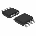 NTMD3P03R2

The activity of extra discounts on wholesale prices is in full swing…
Please fill in your contact information and we will send you the latest wholesale price list.





