 ChipApex | Global Electronic Components Supplier

SEARCH
Search Product
Search Post
— IC芯片 | 连接器 | 传感器 | 被动器件 —
Search productSearch post
— IC芯片 | 连接器 | 传感器 | 被动器件 —
Consult the customer manager about the wholesale price.
consultation hotline:86-132-6715-2157
email:[email protected]
Contact the product manager for consultation. One-stop consultation is available.
Do you want a lower wholesale price? Please send us your inquiry and we will reply immediately.
The NTZD3156CT2G is a dual N/P-channel enhancement mode MOSFET array manufactured by onsemi. It is housed in a surface-mount SOT-563 package with six pins. The device features a maximum drain-source voltage of 20 V. Continuous drain current ratings are specified at 450 mA for the N-channel and 570 mA for the P-channel. The maximum on-resistance values are 2 Ω for the N-channel and 900 mΩ for the P-channel. The gate threshold voltage reaches a maximum of 1 V. Maximum power dissipation is rated at 280 mW, with an operating temperature range from -55 °C to +150 °C.
Verify the specific suffix 'CT2G' against official manufacturer documentation to confirm tape and reel packaging specifications. Ensure the component meets RoHS compliance standards as indicated by the 'G' suffix. Cross-reference the part number with authorized distributors to validate authenticity and traceability before procurement.
Select this component when a compact dual-switch solution is required for low-voltage systems. Verify that the 20 V rating aligns with the system's maximum supply voltage. Confirm that the thermal dissipation capabilities of the SOT-563 package are sufficient for the intended duty cycle and ambient temperature conditions.
This part belongs to onsemi's portfolio of small-signal MOSFET arrays. It serves as a discrete alternative to integrated load switch ICs, offering flexibility in circuit design. The SOT-563 package allows for space-constrained designs common in portable electronics and mobile devices.
Consult official substitution guides for verified equivalents. Generic cross-references may not match the specific electrical characteristics or pinout configuration of the NTZD3156CT2G.
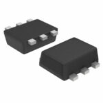 NTZD3156CT2G

The activity of extra discounts on wholesale prices is in full swing…
Please fill in your contact information and we will send you the latest wholesale price list.





