 ChipApex | Global Electronic Components Supplier

SEARCH
Search Product
Search Post
— IC芯片 | 连接器 | 传感器 | 被动器件 —
Search productSearch post
— IC芯片 | 连接器 | 传感器 | 被动器件 —
Consult the customer manager about the wholesale price.
consultation hotline:86-132-6715-2157
email:[email protected]
Contact the product manager for consultation. One-stop consultation is available.
Do you want a lower wholesale price? Please send us your inquiry and we will reply immediately.
The NVTJD4001NT1G is a dual N-channel small signal MOSFET in an SC-88 (SOT-363) package. It features a drain-to-source voltage of 30 V and a continuous drain current of 250 mA at 25 °C. The device has a maximum power dissipation of 272 mW and operates within a junction temperature range of -55 °C to 150 °C. Electrical characteristics include a typical on-resistance of 1.0 Ω at VGS = 4.0 V and 1.5 Ω at VGS = 2.5 V, with a total gate charge of 0.9 nC.
Verify the specific ordering suffix 'NT1G' corresponds to the tape and reel packaging configuration required for automated assembly processes. Confirm that the AEC-Q101 qualification status aligns with automotive reliability standards if the application environment demands it. Ensure the SC-88 package dimensions match the target PCB land pattern specifications.
Select this component when a compact dual N-channel solution is required for low-voltage logic interfacing or power management. The low gate charge supports efficient operation in high-frequency switching applications. Verify that the 30 V rating provides sufficient headroom for the specific circuit supply voltages and transient conditions encountered during normal operation.
This part belongs to the NTJD4001N family of dual N-channel MOSFETs manufactured by onsemi. The 'V' prefix indicates AEC-Q101 qualification for automotive applications. It serves as a space-efficient alternative to larger packages like TSOP-6 while maintaining comparable electrical performance for small-signal switching tasks.
Direct substitutes include the NTJD4001NT1G and NSTJD4001NT1G variants from the same manufacturer family.
Pin 1 is Source 1, Pin 2 is Gate 1, Pin 3 is Drain 2, Pin 4 is Source 2, Pin 5 is Gate 2, and Pin 6 is Drain 1.
Yes, the NVTJD4001N variant is qualified according to the AEC-Q101 standard.
The maximum pulsed drain current is 600 mA with a pulse width of 10 microseconds.
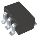 NVTJD4001NT1G

The activity of extra discounts on wholesale prices is in full swing…
Please fill in your contact information and we will send you the latest wholesale price list.





