 ChipApex | Global Electronic Components Supplier

SEARCH
Search Product
Search Post
— IC芯片 | 连接器 | 传感器 | 被动器件 —
Search productSearch post
— IC芯片 | 连接器 | 传感器 | 被动器件 —
Consult the customer manager about the wholesale price.
consultation hotline:86-132-6715-2157
email:[email protected]
Contact the product manager for consultation. One-stop consultation is available.
Do you want a lower wholesale price? Please send us your inquiry and we will reply immediately.
PCA9512ADP,118 is listed in the Signal Buffers, Repeaters, Splitters range at ChipApex. The manufacturer field lists NXP USA Inc.. Its product description is IC ACCELERATR I2C HOTSWAP 8TSSOP. Review the specifications below when checking this part for your BOM.
The PCA9512ADP,118 is a hot swappable I2C-bus and SMBus buffer in an 8-lead TSSOP package. It provides bidirectional buffering for SDA and SCL lines to increase fan-out and prevent bus corruption during live board insertion. The device features two dedicated supply voltage pins (VCC and VCC2) supporting level shifting between 3.3 V and 5 V systems within a 2.7 V to 5.5 V operating range. It includes built-in ΔV/Δt rise time accelerators with a 0.6 V threshold, 1 V precharge circuitry, and an ACC pin to disable accelerators. Operating temperatures range from -40 °C to +85 °C.
Verify the specific ordering suffix '118' corresponds to the reel packing method required for your assembly line. Confirm that the TSSOP8 package dimensions align with your PCB footprint design rules. Ensure the component temperature rating meets your system's operational environment requirements before finalizing procurement.
Select this part when dual-supply level shifting is required alongside hot swap protection. The PCA9512A supports both Standard-mode and Fast-mode I2C standards up to 400 kHz. Consider the ACC pin functionality if your system requires disabling rise time accelerators for lightly loaded buses to minimize power consumption or signal overshoot.
This component belongs to the PCA9512A family of level-shifting bus buffers. The ADP suffix specifically denotes the TSSOP8 plastic thin shrink small outline package variant. Other family members include the PCA9510A through PCA9514A, which offer varying feature sets such as different rise time accelerator thresholds or ready outputs.
Direct replacements within the same package and feature set are limited due to specific level-shifting capabilities. Verify compatibility with PCA9512AD variants if SO8 packaging is acceptable. Cross-referencing with PCA9511A or PCA9513A may be necessary if specific features like READY outputs or different accelerator thresholds are required.
Control circuitry prevents the backplane from connecting to the card until a stop bit or bus idle condition occurs, ensuring no bus contention arises during the connection process.
The ACC pin is a digital input that enables or disables the rise time accelerators. Driving it to VCC2 enables normal operation, while driving it to GND turns off the accelerators for lightly loaded systems.
Yes, either VCC or VCC2 may be powered first, and they can have different voltage levels within the 2.7 V to 5.5 V range, allowing for flexible level shifting configurations.
Explore related parts through Interface, Integrated Circuits (ICs), all product categories, ChipApex homepage.
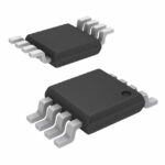 PCA9512ADP,118
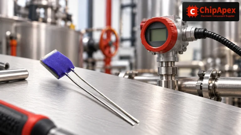
Compare Pt100 and Pt1000 RTDs, two-, three- and four-wire connections, excitation and self-heating. Build an error budget from element to reported temperature.
Read More
PCA9512ADP,118 is listed in the Signal Buffers, Repeaters, Splitters range at ChipApex. The manufacturer field lists NXP USA Inc.. Its product description is IC…
Read More
PCA9512ADP,118 is listed in the Signal Buffers, Repeaters, Splitters range at ChipApex. The manufacturer field lists NXP USA Inc.. Its product description is IC…
Read More
PCA9512ADP,118 is listed in the Signal Buffers, Repeaters, Splitters range at ChipApex. The manufacturer field lists NXP USA Inc.. Its product description is IC…
Read More
Choose an AC to DC converter by input range, output demand, isolation, efficiency and thermal derating. Compare architectures and check installation needs.
Read More
PCA9512ADP,118 is listed in the Signal Buffers, Repeaters, Splitters range at ChipApex. The manufacturer field lists NXP USA Inc.. Its product description is IC…
Read More
PCA9512ADP,118 is listed in the Signal Buffers, Repeaters, Splitters range at ChipApex. The manufacturer field lists NXP USA Inc.. Its product description is IC…
Read More
See how a MEMS gyroscope measures angular rate, why its angle estimate drifts, and which range, noise, interface and temperature specs to compare.
Read More
PCA9512ADP,118 is listed in the Signal Buffers, Repeaters, Splitters range at ChipApex. The manufacturer field lists NXP USA Inc.. Its product description is IC…
Read More
PCA9512ADP,118 is listed in the Signal Buffers, Repeaters, Splitters range at ChipApex. The manufacturer field lists NXP USA Inc.. Its product description is IC…
Read More
PCA9512ADP,118 is listed in the Signal Buffers, Repeaters, Splitters range at ChipApex. The manufacturer field lists NXP USA Inc.. Its product description is IC…
Read More
PCA9512ADP,118 is listed in the Signal Buffers, Repeaters, Splitters range at ChipApex. The manufacturer field lists NXP USA Inc.. Its product description is IC…
Read More
The activity of extra discounts on wholesale prices is in full swing…
Please fill in your contact information and we will send you the latest wholesale price list.





