 ChipApex | Global Electronic Components Supplier

SEARCH
Search Product
Search Post
— IC芯片 | 连接器 | 传感器 | 被动器件 —
Search productSearch post
— IC芯片 | 连接器 | 传感器 | 被动器件 —
Consult the customer manager about the wholesale price.
consultation hotline:86-132-6715-2157
email:[email protected]
Contact the product manager for consultation. One-stop consultation is available.
Do you want a lower wholesale price? Please send us your inquiry and we will reply immediately.
The PHN210T is a dual intermediate level N-channel enhancement mode Field-Effect Transistor utilizing TrenchMOS technology in an SO8 plastic package. It features a drain-source voltage of 30 V and a continuous drain current of 3.4 A at 25 °C. The on-state resistance ranges from 80 mΩ to 200 mΩ depending on gate drive conditions. Total power dissipation is rated at 2 W, with a junction temperature range of -65 °C to 150 °C.
Verify the specific ordering suffix against the manufacturer's current catalog to ensure correct packaging configuration. Confirm that the application environment remains within the specified non-automotive scope, as this component lacks automotive qualification. Cross-reference thermal management requirements with the provided transient thermal impedance data before finalizing the design.
Select this component for designs requiring dual N-channel switching in a compact surface-mount footprint. Ensure the gate drive circuitry aligns with the intermediate level threshold specifications. Evaluate the thermal resistance parameters against the expected ambient temperature and duty cycle to maintain junction temperatures within safe operating limits during continuous operation.
This device belongs to Nexperia's TrenchMOS portfolio, designed for computing, communications, consumer, and industrial sectors. It integrates two independent N-channel FETs into a single SO8 package to save board space. The technology focuses on balancing conduction losses with switching speed for general-purpose power control tasks.
Consult official substitution guides for equivalent dual N-channel MOSFETs in SOT96-1 packages. Verify pin compatibility and electrical parameter overlaps before swapping components in existing layouts.
No, the product data sheet explicitly states it is designed for computing, communications, consumer, and industrial applications only.
The maximum repetitive peak drain-source voltage is 30 V.
The SO8 plastic small outline package contains 8 leads.
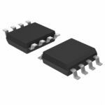 PHN210T,118

The activity of extra discounts on wholesale prices is in full swing…
Please fill in your contact information and we will send you the latest wholesale price list.





